| Posted: Oct 18, 2006 |
Nanocoating woodfibers results in smart paper |
| (Nanowerk Spotlight) Paper manufacturing is one of the mainstays of economic infrastructure and paper products influence many aspects of business and personal life. Pulping, process chemistry, paper coating, and recycling are key areas that can benefit from nanotechnology methods. One such method, layer-by-layer (LbL) assembly, is of great interest of its usage in the field of nanocoating. It allows creating nanometer-sized ultrathin films both on large surfaces and on microfibers and cores with the desired composition. Researchers at Louisiana Tech University have developed a simple and cost effective technique to fabricate an electrically conductive paper by applying layer-by-layer nanoassembly coating directly on wood microfibers during paper making process. Nanocoated wood microfibers and paper may be applied to make electronic devices, such as capacitors, inductors, and transistors fabricated on cost-effective lignocellulose pulp. The use of a conductive nanocoating on wood fibers can open the door for the future development of smart paper technology, applied as sensors, communication devices, electromagnetic shields, and paper-based displays. |
| Dr. Mangilal Agarwal, Dr. Yuri Lvov and Dr. Kody Varahramyan reported their novel process in a paper, titled "Conductive wood microfibers for smart paper through layer-by-layer nanocoating", that was published in the October 6, 2006 online edition of Nanotechnology. |
| Agarwal, who is a researcher at the Institute for Micromanufacturing at Louisiana Tech, explains the new process to Nanowerk: "In this work we have demonstrated successful scale integration from nano to micro and macroscale (nanocoating - microfibers - macropaper) in developing new paper material. The conductive paper that has been produced (and its fabrication method) can be used for the development of smart paper technology or functional textiles." |
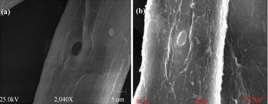 |
| SEM micrograph of the wood microfibers. (a) Uncoated microfiber; (b) microfibers coated with four bilayers of PEI and PEDOT–PSS polymers. (Reprinted with permission from IOP Publishing) |
| The researchers used an aqueous dispersion of anionic poly(3,4-ethylenedioxythiophene) – poly(styrenesulfonate) (PEDOT–PSS) and poly(allylamine hydrochloride) (PAH) and poly(ethyleneimine) (PEI) as their cationic polyelectrolytes for LbL assembly. By creating organized multilayers of these polyelectrolytes on a surface of wood microfibers, they have produced a nanocoating that enables the microfibers to exhibit moderate electrical conductivity, which was increased by increasing the number of conductive polymer layers in the coating. Subsequently, they used these fibers for the production of handsheets that have a measurable electrical conductivity. |
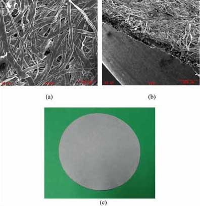 |
| (a) SEM micrograph of the handsheet prepared using wood microfibers coated with four layers of PEDOT–PSS alternating with PEI; (b) SEM micrograph of the handsheet edge (SEM AMREY-1830); (c) photographic image of the full handsheet of 6 inch diameter. (Reprinted with permission from IOP Publishing) |
| Agarwal points out that LbL nanoassembled conductive coating on wood microfibers could be useful in many ways. The nanoassembly approach to coat electrically or optically active polymers directly on wood fibers (during the paper making process) is cost effective, simple and superior to other techniques where the coating is done after the formation of final paper product. Also, the approach is environmentally friendly due to the use of aqueous dispersion of polymer materials in the coating process. |
| "Using this technique, we are looking forward to create electronic devices for displays, switches, filters, interconnects, actuators, biological, chemical and environmental sensors that can be integrated into paper" he says. |
| This technique is very promising and cost effective for applications like large paper-based displays, smart cards (greeting cards, business cards, etc.), and paper products with embedded electronic/optical signature. This approach can be used to embed electrical/optical signature into money (currency notes) and other security documents to avoid counterfeiting. Also, large paper-based electromagnetic shield for both domestic and military applications, and Radio Identification Tags (RFID) as a route to smart packaging and logistic tracking in retail stores and warehouses can be realized. |
| "Our goal is to make electrical/optically active paper-based products to avoid counterfeiting and also make paper-based electromagnetic shields which can be used for communication applications" says Agarwal. "On the other hand, we are integrating chemical, biological and environmental sensors embedded into the paper, which can be used in both domestic and defense applications." |
| Dr. Agarwal can be reached at the Institute for Micromanufacturing at Louisiana Tech University, Email: [email protected], Ph: 318-614-5430, Fax: 318-257-5104. |
 By
Michael
Berger
– Michael is author of four books by the Royal Society of Chemistry:
Nano-Society: Pushing the Boundaries of Technology (2009),
Nanotechnology: The Future is Tiny (2016),
Nanoengineering: The Skills and Tools Making Technology Invisible (2019), and
Waste not! How Nanotechnologies Can Increase Efficiencies Throughout Society (2025)
Copyright ©
Nanowerk LLC
By
Michael
Berger
– Michael is author of four books by the Royal Society of Chemistry:
Nano-Society: Pushing the Boundaries of Technology (2009),
Nanotechnology: The Future is Tiny (2016),
Nanoengineering: The Skills and Tools Making Technology Invisible (2019), and
Waste not! How Nanotechnologies Can Increase Efficiencies Throughout Society (2025)
Copyright ©
Nanowerk LLC
|

Become a Spotlight guest author! Join our large and growing group of guest contributors. Have you just published a scientific paper or have other exciting developments to share with the nanotechnology community? Here is how to publish on nanowerk.com.
