| Posted: Oct 27, 2006 |
Novel method simplifies large-scale nanofabrication process |
| (Nanowerk Spotlight) As scientific interests and engineering applications delve down to the nanometer scale, there is a strong need to fabricate nanostructures with good regularity and controllability of their pattern, size, and shape. Furthermore, the nanostructures are useful in many applications only if they cover a relatively large sample area and the manufacturing cost is reasonable. |
| Researchers at UCLA have now achieved a breakthrough by developing a simple but efficient fabrication method to produce well-regulated silicon nanostructures over a large sample area with excellent control of their pattern, size, and shape. Affordable surfaces with well-controlled nanostructures over a large area open new applications not only in electronics but also in the physical world through their unique properties originating from their nanoscale geometry. |
| While several nanoscale patterning techniques are known and available, most of them involve a serial method such as e-beam lithography inapt for covering areas larger than squre millimeters. X-ray lithography is parallel and can pattern a large area, but it is too expensive for most applications. Soft lithography-based fabrication, such as nanoimprinting, replicates patterns in a parallel fashion, but it still needs a master mold first manufactured by e-beam or X-ray lithography. Most non-lithographic methods, such as the use of nanotemplates (e.g., copolymers) or the direct growth of nanostructures (e.g., carbon nanotubes), lack the regularity some applications demand over a large area. |
| Professor Chang-Jin "CJ" Kim and Chang-Hwan Choi from the Micro- and Nanomanufacturing Laboratory at UCLA's Mechanical and Aerospace Engineering Department, came up with a simple but efficient nanofabrication method to create a dense (nanoscale pitch) array of silicon nanostructures (post and grate) of varying height and shape over a large sample area. |
| Choi explained their findings to Nanowerk: "We coupled interference lithography with deep reactive ion etching (DRIE), which is a new nanofabrication approach. Interference lithography is currently considered the most efficient way to make submicron-scale periodic patterns over a large area (up to a meter range, reportedly) with excellent control of pattern regularity. Although DRIE has rarely been used to construct nanostructures because the rippling of sidewalls (so-called ‘scalloping effect’) is too prominent on the nanoscale, we demonstrated that a common DRIE process could produce well-defined tall nanostructures by controlling etching parameters and even tailor the sidewall profiles of the nanostructures as desired." |
| The new idea of utilizing the DRIE and the nanoscale scalloping effect inherent in it for nanostructure fabrication not only simplified nanofabrication processes but also enabled three-dimensional nanofabrication with a single lithography and etching step. |
| "If conventional techniques were used to create the structures similar to ours, multiple lithography steps with precise alignment or a lithography step with multi-layer resists (or multi-step post processes) would have been required" says Choi. "The three-dimensional sidewall profile control further enabled a simple way to subsequently sharpen the nanostructures’ tips for pointed sharp-tip nanostructures." |
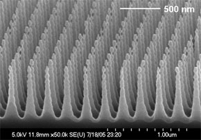 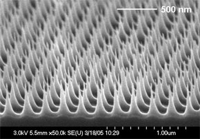 |
(Left) SEM image of a silicon nanopost structure with the three-dimensional variation of the sidewall profile enabled by modulating the nanoscalloping effect in DRIE. (Right) SEM image of silicon nanostructures nanostructures with sharp tips. Tips of nanostructures whose sidewall profiles were designed to be positively tapered and scalloping-free were subsequently sharpened by thermal oxidation followed by oxide etching, and measure less than 5 nm in tip apex radius of curvature. (Source: Chang-Hwan Choi) |
| The researchers point out that three-dimensional nanostructures such as a re-entrant sidewall profile (such re-entrant sidewall profiles are not shown here but can be seen in their recent report "Fabrication of a dense array of tall nanostructures over a large sample area with sidewall profile and tip sharpness control" in the October 6, 2006 online edition of Nanotechnology) are desirable in several applications, such as T-gates for microwave transistors, wave modulators for nano-optics, and various nanoelectromechanical systems (NEMS). |
| For a given void fraction under the surface, nanostructures with a re-entrant profile provide less open and more flat area on the surface than simple profiles do. Another use of such a re-entrant profile would be to produce monolithic nanochannels by sealing the top of the nanograte patterns with a thin-film deposition. |
| Well-regulated sharp-tip nanostructures covering a large pattern area, especially needle-like nanopost patterns, commonly are of interest in such electronic applications as field emitter structures. The simple but efficient method of sharp-tip nanofabrication will also facilitate the design and fabrication of high-aspect-ratio scanning probe tips. |
| "Our first application opened by the densely-populated nanostructures over a large sample area was to fabricate nanopatterned superhydrophobic surfaces of good mechanical robustness and geometric regularity, compared with the micropatterned or irregularly-patterned (e.g., chemically-formed or polymer-roughened) superhydrophobic surfaces that have so far been reported" says Choi. "The nanostructures with the regular pitch and shape allowed us to study the effect of nanostructure geometries on the surface superhydrophobicity." |
| Especially, slender and tall sharp-tip nanostructures with the nanometer-scale dense pitch made the microfluidic application to the friction reduction in liquid flow more practical and beneficial, tolerating highly pressurized flows without losing the superhydrophobicity. These findings were reported in Physical Review Letters ("Large Slip of Aqueous Liquid Flow over a Nanoengineered Superhydrophobic Surface") and Physics of Fluids ("Effective slip and friction reduction in nanograted superhydrophobic microchannels"). |
| Choi notes that the well-regulated nanotopographical properties of their nanostructures enabled another possibility for exploration, which is cell biology. Although several cell behaviors over various surface topographies have been studied with micro- and nanostructured surfaces, there is little information on the cell reactions to the well-ordered nanostructured surfaces. |
| "Our well-ordered nanostructures provided a unique opportunity, whereby the well-defined surface structures on the nanoscale could elucidate many aspects of the nanobiology of the cell, including the effect of surface three-dimensionality (i.e., three-dimensional nanotopography) on cell proliferation, morphology, alignment, and adhesion, whose understanding will further be utilized for cell and tissue engineering applications" he says. (Further details can be found in a recent paper "Cell Adhesions on Nanoturf Surfaces", which appeared in Proceedings of the 19th International Conference on Micro Electro Mechanical Systems, Istanbul, Turkey). |
| Currently, the nanostructured surface fabricated at Kim's lab is made out of a silicon substrate. Well-regulated nanostructures of other materials such as soft polymers are also desired for certain applications, e.g., novel biomaterials for tissue engineering. Nanopatterned soft polymer materials will also have superiority to rigid solid nanostructured surfaces in respect that they can create a flexible nanostructured surface and be applied on curved bodies. |
| The DRIE is not suitable to etch the other material than silicon so that new nanofabrication methods for the flexible soft materials may need to be sought in the future. |
| "To retain the advantage of the current method – good control of pattern, size, and shape – our well-regulated silicon nanostructures can be used as mold or master structures to be replicated on the soft materials, which is now investigated in our lab" Choi concludes. |
 By
Michael
Berger
– Michael is author of four books by the Royal Society of Chemistry:
Nano-Society: Pushing the Boundaries of Technology (2009),
Nanotechnology: The Future is Tiny (2016),
Nanoengineering: The Skills and Tools Making Technology Invisible (2019), and
Waste not! How Nanotechnologies Can Increase Efficiencies Throughout Society (2025)
Copyright ©
Nanowerk LLC
By
Michael
Berger
– Michael is author of four books by the Royal Society of Chemistry:
Nano-Society: Pushing the Boundaries of Technology (2009),
Nanotechnology: The Future is Tiny (2016),
Nanoengineering: The Skills and Tools Making Technology Invisible (2019), and
Waste not! How Nanotechnologies Can Increase Efficiencies Throughout Society (2025)
Copyright ©
Nanowerk LLC
|

Become a Spotlight guest author! Join our large and growing group of guest contributors. Have you just published a scientific paper or have other exciting developments to share with the nanotechnology community? Here is how to publish on nanowerk.com.
