| Posted: Aug 27, 2014 |
New DARPA 'Atoms to Product' program seeks to develop advanced nanotechnology
|
|
(Nanowerk News) Many common materials exhibit different and potentially useful characteristics when fabricated at extremely small scales—that is, at dimensions near the size of atoms, or a few ten-billionths of a meter. These “atomic scale” or “nanoscale” properties include quantized electrical characteristics, glueless adhesion, rapid temperature changes, and tunable light absorption and scattering that, if available in human-scale products and systems, could offer potentially revolutionary defense and commercial capabilities. Two as-yet insurmountable technical challenges, however, stand in the way: Lack of knowledge of how to retain nanoscale properties in materials at larger scales, and lack of assembly capabilities for items between nanoscale and 100 microns—slightly wider than a human hair.
|
|
DARPA has created the Atoms to Product (A2P) program to help overcome these challenges. The program seeks to develop enhanced technologies for assembling atomic-scale pieces. It also seeks to integrate these components into materials and systems from nanoscale up to product scale in ways that preserve and exploit distinctive nanoscale properties.
|
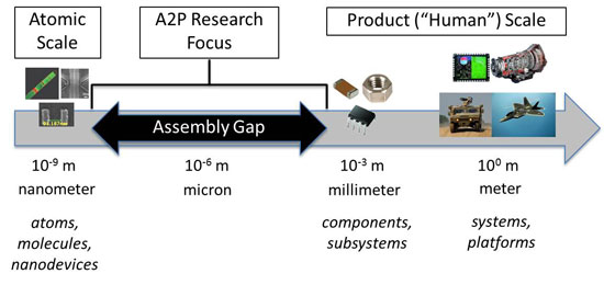 |
| DARPA’s Atoms to Product (A2P) program seeks to develop enhanced technologies for assembling nanoscale items, and integrating these components into materials and systems from nanoscale up to product scale in ways that preserve and exploit distinctive nanoscale properties.
|
|
“We want to explore new ways of putting incredibly tiny things together, with the goal of developing new miniaturization and assembly methods that would work at scales 100,000 times smaller than current state-of-the-art technology,” said John Main, DARPA program manager. “If successful, A2P could help enable creation of entirely new classes of materials that exhibit nanoscale properties at all scales. It could lead to the ability to miniaturize materials, processes and devices that can’t be miniaturized with current technology, as well as build three-dimensional products and systems at much smaller sizes.”
|
|
This degree of scaled assembly is common in nature, Main continued. “Plants and animals, for example, are effectively systems assembled from atomic- and molecular-scale components a million to a billion times smaller than the whole organism. We’re trying to lay a similar foundation for developing future materials and devices.”
|
|
To familiarize potential participants with the technical objectives of the A2P program, DARPA has scheduled identical Proposers Day webinars on Tuesday, September 9, 2014, and Thursday, September 11, 2014. Advance registration is required and closes on September 5, 2014, at 5:00 PM Eastern Time.
|
|
The DARPA Special Notice announcing the Proposers’ Day webinars is available at go.usa.gov/mgKB. This announcement does not constitute a formal solicitation for proposals or abstracts and is issued solely for information and program planning purposes. The Special Notice is not a Request for Information (RFI); therefore, DARPA will accept no submissions against this announcement. DARPA expects to release a Broad Agency Announcement (BAA) with full technical details on A2P soon on the Federal Business Opportunities website (www.fbo.gov). For more information, please email [email protected].
|