| Apr 26, 2024 |
Breakthroughs in optical modulation using tunable 2D materials
(Nanowerk News) Tunable optical materials (TOMs) are revolutionizing modern optoelectronics. In integrated photonics circuits, precise control over the effective refractive index is crucial for unlocking groundbreaking applications. Two-dimensional materials such as Transition Metal Dichalcogenides (TMDs) and graphene offer exceptional optical responses to external stimuli. Yet, achieving distinct modulation across the short-wave infrared (SWIR) region, while maintaining precise phase control with minimal signal loss in a compact footprint, remains a persistent challenge.
|
|
In a new paper published in Light Science & Application ("Electro-optic tuning in composite silicon photonics based on ferroionic 2D materials"), a team of scientists, led by Dr Ghada Dushaq and Professor Mahmoud Rasras Photonic Research Lab, Department of Electrical and Computer Engineering, New York University Abu Dhabi, Abu Dhabi, United Arab Emirates and co-workers have demonstrated a novel avenue for active light manipulation through the utilization of ferroionic 2D CCPS material.
|
 |
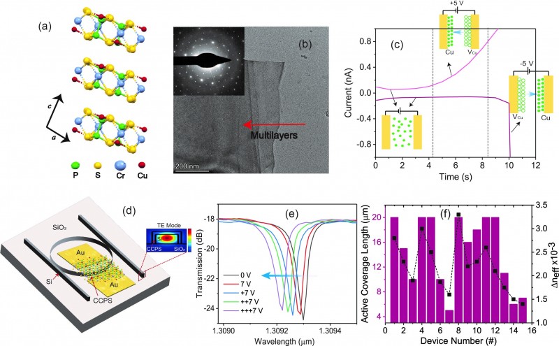
| (a) 3D schematic visualization (ball and stick model) of a-c plane in CCPS structure, (b) Transmission electron microscopy (TEM) image along with the selected area diffraction pattern (SADP) of CCPS crystal, (c) current- time (I-t) characteristics at ± 5 V along with a schematic representation of Cu distribution, (d) 3D schematic representation of the Si microring resonator (MRR) design with integrated CCPS, (e) the transmission spectra of MRR at a constant voltage of 7 V as the polling time progressed, across all scans, a consistent blue shift in the resonance wavelengths was observed for all fabricated devices. This blue shift implies an electro-optical modulation of the refractive index of the combined Si/CCPS guiding structure, given that thermal heating typically results in a red shift in the Si-MRR resonance wavelength, additionally, the application of a bias across the device does not affect the extinction ratios and the resonance linewidth, (f) coverage length and change in effective refractive index of the 15 tested devices. (Image: Light Science & Application) (click on image to enlarge)
|
|
When integrated onto SiPh microring resonators, these materials exhibit a remarkable ability to finely tune the effective index of refraction without any attenuation of the optical signal. Remarkably, these integrated devices showcase low optical losses and exhibit an exceptional modulation efficiency (Vπ. L) of 0.25 V·cm, coupled with a consistent blue shift in resonance wavelengths across all devices.
|
|
The ability to actively manipulate the electro-optic response in 2D CCPS at near-infrared wavelengths presents a pathway to more efficient and versatile optoelectronic devices, with implications spanning telecommunications, neuromorphic computing, and beyond.
|
|
The robust electro-refractive response of these devices hinges on the electronic properties of ferroionic 2D CCPS, significantly impacted by their bulk ionic conductivity. This pivotal aspect can be finely tuned through the manipulation of factors like poling time, polarization, and current direction. Such adjustments influence the migration of highly mobile copper (Cu) ions, underscoring the interconnected nature of material properties and device performance. These scientists summarize the operational principle of their devices:
|
|
“We have demonstrated a novel approach for actively manipulating light by employing ferroionic 2D CCPS material. Integrated into SiPh microring resonators, these materials showcase an exceptional ability to precisely adjust the effective refractive index without introducing any amplitude chirp. This capability is attributed to the tunable electrical conduction arising from the reversible migration of mobile Cu ions at the metal-semiconductor interface. The flexibility of the Cu–S bond facilitates Cu ion hopping between intralayer and interlayer sites, and even across the van der Waals (vdW) gap under an electric field. Consequently, optical tuning is achieved through the reversible process of extracting Cu ions from sulfur octahedra across van der Waals gaps and their reintercalation into the layers, a process that is reliably controlled by the applied voltage.”
|
|
“Remarkably, the application of a bias across the device does not affect the extinction ratios and the resonance linewidth. Therefore, the active migration of Cu ions has no impact on the imaginary part of the refractive index” they added.
|
|
“The combined optoelectronic and ionotronic functionalities in the two-terminal CCPS device hold potential for applications, including phased arrays, optical switching, environmental sensing and metrology, optical imaging systems, and neuromorphic systems in light-sensitive artificial synapses.” the scientists forecast.
|