| Posted: Oct 27, 2014 |
Researcher develop economical process for micro energy harvesting
|
|
(Nanowerk News) The trend toward energy self-sufficient probes and ever smaller mobile electronics systems continues unabated. They are used, for example, to monitor the status of the engines on airplanes, or for medical implants. They gather the energy they need for this from their immediate environment - from vibrations, for instance. Fraunhofer researchers have developed a process for the economical production of piezoelectric materials. They will unveil a preliminary demonstration model at this year’s electronica trade show from November 11 to 14 in Munich (Hall A4, Booth 113).
|
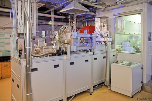 |
| Fraunhofer researchers are using this lab coater to produce piezoelectric AlN layers for low power sensors in an economically feasible manner. (Image: Fraunhofer FEP)
|
|
When there is little space, or an exchange is complicated, then power supply for sensors via battery or cable is most often too circuitous. The best approach is to have the energy intake integrated and highly durable. One solution is offered by Energy Harvesting – onsite power production for instance through solar cells, thermoelectric or piezoelectric materials.
|
|
Piezoelectric materials can convert mechanical vibrations into electric energy because the effect of mechanical force results in a charge separation. They can be applied in places where a defined but not necessarily constant state of vibration exists – on industrial equipment, for example, or airplane engines, in car engines or even on the human body, where blood pressure, breathing or heartbeat are constantly creating momentum. Up to now, the piezoelectric material of choice has mainly been leadzirconium- titanium composites (PZT). Aluminum nitride (AlN) is another option. Compared to PZT, it possesses more favorable mechanical properties, is lead-free, more stable and biocompatible. Moreover, it is virtually no problem to integrate AlN layers into conventional manufacturing processes for microelectronics.
|
|
New process for manufacturing piezo coatings
|
|
Here’s the dilemma: In order to integrate piezoelectric materials into increasingly smaller electrical systems, they likewise have to be as small as possible - on the one hand. On the other hand, they need a certain volume in order to produce sufficient energy. So far it has been impossible to produce the targeted coatings in a manner that is economically feasible enough using the available methods to date. Deposition rates, homogeneity and coating areas are too small. But now, scientists at Fraunhofer Institute for Organic Electronics, Electron Beam and Plasma Technology FEP have developed a process by which they can precipitate highly homogeneous layers on diameters of up to 200 mm with simultaneously high deposition rates. Thus, the process is substantially more productive and profitable than previous processes.
|
|
The researchers deposited the layers by reactive magnetron sputtering of aluminum targets in an argon-nitrogen atmosphere onto a silicon wafer. With this physical procedure, atoms from solid bodies are discharged into the gas phase by bombarding the targets with highly energetic noble gas ions. They then deposit on the wafer as a layer. For this purpose, the FEP scientists use the DRM 400, a double ring magnetron sputter source developed in-house that consists of two ring-shaped targets. Since the discharges of both targets overlap, it is possible to deposit the AlN layers homogeneously onto a large coating surface with a piezo-coefficient d33 of up to 7 pC/N. The higher this figure, the more strongly the material reacts. The typical values described in available research literature for the piezo-coefficient d33 of AlN ranges between 5 to 7 pC/N. At the same time, the mechanical stress of the layers can be flexibly modified to the relevant field of application. These impact for example the adhesion strength of the coating, the electromechanical coupling and the values of the energy produced.
|
|
Boosting energy yields even further
|
|
Working in collaboration with the Technical University of Dresden and Oulu University in Finland, the FEP researchers conducted tests on energy harvesting with AlN coatings on silicon strips measuring 6x1cm2. For demonstrations, they were able to reach generated powers of several hundred µW. According to project manager Stephan Barth, this figure admittedly cannot be transferred to a practical application at a 1:1 ratio, since the generated power depends on multiple factors: “On the one hand, the design – that is to say the layer thickness, transducer geometry, volume, space and substrate materials all have an impact; on the other hand, there is an effect from the vibrational behavior, such as frequency, amplitude or ambient medium and one should also keep in mind the necessity of the matching to the sensor electronics." Nonetheless, the AlN layers are a practicable alternative for operating low-power sensors, as they are used in industrial applications or with cardiac pacemakers.
|
|
In order to raise the power yield even higher, scientists are additionally using layers made from aluminum-scandium-nitride, which they deposit by reactive co-sputtering. Compared to pure AlN, these exhibit substantially higher piezo-coefficients with similar coating rates. This means three to four times more power is produced through this. Another future focus of the researchers’ work will be placed on optimization of the transducer design for power production. The goal would be to downsize the entire construction, to elevate capacities even further, and to better adapt resonance frequency to the respective application.
|