| Posted: Nov 20, 2014 |
Tomorrow's degradable electronics
|
|
(Nanowerk News) When the FM frequencies are removed in Norway in 2017, all old-fashioned radios will become obsolete, leaving the biggest collection of redundant electronics ever seen – a mountain of waste weighing something between 25,000 and 30,000 tonnes.
|
|
The same thing is happening with today’s mobile telephones, PCs and tablets, all of which are constantly being updated and replaced faster than the blink of an eye. The old devices end up on waste tips, and even though we in the west recover some materials for recycling, this is only a small proportion of the whole.
|
|
And nor does the future bode well with waste in mind. Technologists’ vision of the future is the “Internet of Things”. Electronics are currently printed onto plastics. All products are fitted with sensors designed to measure something, and to make it possible to talk to other devices around them. Davor Sutija is General Manager at the electronics firm Thin Film, and he predicts that in the course of a few years each of us will progress from having a single sensor to having between a hundred and a thousand. This in turn will mean that billions of devices with electronic bar codes will be released onto the market.
|
 |
| Electronic circuits can be implanted into surgical wounds and assist the healing process by accelerating wound closure. After a few weeks, the electronics are dissolved by the body fluids, making it unnecessary to re-open the wound to remove them manually. (Image: Werner Juvik/SINTEF)
|
|
No time to lose
|
|
Researchers are now getting to grips with this problem. Their aim is to develop processes in which electronics are manufactured in such a way that their entire life cycle is controlled, including their ultimate disappearance.
|
|
In New Orleans in the USA, researchers have made electronic circuits which they implant into surgical wounds following operations on rats. Each wound is sewn up and the electricity in the circuits then accelerates the healing process. After a few weeks, the electronics are dissolved by the body fluids, making it unnecessary to re-open the wound to remove them manually.
|
|
In Norway, researchers at SINTEF have now succeeded in making components containing magnesium circuits designed to transfer energy. These are soluble in water and disappear after a few hours.
|
|
A demanding process
|
|
“We make no secret of the fact that we are putting our faith in the research results coming out of the USA”, says Karsten Husby at SINTEF ICT. “The Americans have made amazing contributions both in relation to medical applications, and towards resolving the issue of waste. We want to try to find alternative approaches to the same problem”, he says.
|
|
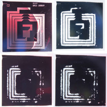
The circuit containing the small components is printed on a silicon wafer. At only a few nanometres thick, the circuits are extremely thin, and this enables them to dissolve more effectively. Some of the circuit components are made of magnesium, others of silicon, and others of silicon with a magnesium additive.
|
|
But the journey to the researchers’ goal from their current position leaves them with more than enough work to do. Making the ultra-thin circuits is a challenge enough in itself, but they also have to find a “coating” or “film” which will act as a protective packaging around the circuits.
|
|
The Americans use silk as their coating material, but the Norwegians are not in favour of this. The silk used is made as part of a process which involves the substance lithium, which is banned at MiNaLab – the laboratory where the SINTEF researchers work.
|
|
“Lithium generates a technical problem for our lab”, says Geir Uri Jensen, “so we’re considering alternatives, including a variety of plastics”, he says. “In order to achieve this, we’ve brought in some materials scientists here at SINTEF who are very skilled in this field”, he says.
|
|
The nature of the coating must be tailored to the time at which the electronics are required to degrade. In some cases this is just one week – in others, four. For example, if the circuit package is designed to be used in seawater, and fitted with sensors for taking measurements from oil spills, the film must be made so that it remains in place for the weeks in which the measurements are being taken.
|
|
“When the external fluids penetrate to the “guts” inside the packaging, the circuits begin to degrade. The job must be completed before this happens”, says Karsten Husby.
|
|
Geir Uri Jensen makes a sketch and explains how the nano researchers use horizontal and vertical etching processes in the lab to deposit all the layers onto the silicon circuits. And then – how they have to etch and lift the circuit loose from the silicon wafer in order later to transfer it across to the film.
|
|
“This works well enough using sensors at full scale”, he says, “but when the wafers are as thin as this, things become more tricky”. Jensen shrugs. “Even if the angle is just a little off, the whole assembly will snap”, he says.
|
|
Spanner in the works
|
|
There’s no doubt that as the use of consumer electronics increases, so too does the need to remove obsolete electronic products. Just think of all the cheap electronics built into children’s toys which are thrown away every year.
|
|
The removal of “outdated electronics” can also be a very labour-intensive process. Every day, surgeons place implants fitted with sensors into our bodies in order to measure everything from blood pressure and pressure on the brain, to how our hip implants are working. Some weeks later they have to operate again in order to remove the electronics.
|
|
But not everyone is interested in the new technologies developing in this field. Electronics companies which manufacture circuits are more interested in selling their products than in investing in research that results in their products disappearing. And companies which rely on recycling for their revenues may regard these new ideas as a threat to their existence.
|
|
Eco-friendly electronics are on the way
|
|
“It’s important to make it clear that we’re not manufacturing a final product, but a demo that can show that an electronic component can be made with properties that make it degradable”, says Husby. “Our project is now in its second year, but we’ll need a partner active in the industry and more funding in the years ahead if we’re to meet our objectives. There’s no doubt that eco-friendly electronics is a field which will come into its own, also here in Norway. And we’ve made it our mission to reach our goals”, he says.
|