| Posted: Jul 27, 2016 | |
How to build nanoelectronic devices atom by atom?(Nanowerk News) In the year 2015, Intel, Samsung and TSMC began to mass-market the 14nm technology called FinFETs. In the same year, IBM, working with Global Foundries, Samsung, SUNY, and various equipment suppliers, announced their success in fabricating 7nm devices. A 7nm silicon channel is about 50 atomic layers and these devices are truly atomic! It is clear that we have entered an era of atomic scale transistors. How do we model the carrier transport in such atomic scale devices? |
|
 One way is to improve existing device models by including more and more parameters. This is called the top-down approach. However, as device sizes shrink, the number of parameters grows rapidly, making the top-down approach more and more sophisticated and challenging. Most importantly, to continue Moore's law, electronic engineers are exploring new electronic materials and new operating mechanisms. These efforts are beyond the scope of well-established device models -- hence significant changes are necessary to the top-down approach. An alternative way is called the bottom-up approach. The idea is to build up nanoelectronic devices atom by atom on a computer, and predict the transport behavior from first principles. By doing so, one is allowed to go inside atomic structures and see what happens from there. The elegance of the approach comes from its unification and generality. Everything comes out naturally from the very basic principles of quantum mechanics and nonequilibrium statistics. The bottom-up approach is complementary to the top-down approach, and is extremely useful for testing innovative ideas of future technologies. In recent decades, several device simulation tools using the bottom-up approach have been developed in universities and software companies. Some examples are McDcal, Transiesta, Atomistic Tool Kit, Smeagol, NanoDcal, NanoDsim, OpenMX, GPAW and NEMO-5. These software tools are capable of predicting electric current flowing through a nanostructure. Essentially the input is the atomic coordinates and the output is the electric current. These software tools have been applied extensively to study emerging electronic materials and devices. |
|
| However, developing such a software tool is extremely difficult. It takes years-long experiences and requires knowledge of and techniques in condensed matter physics, computer science, electronic engineering, and applied mathematics. In a library, one can find books on density functional theory, books on quantum transport, books on computer programming, books on numerical algorithms, and books on device simulation. But one can hardly find a book integrating all these fields for the purpose of nanoelectronic device simulation. | |
|
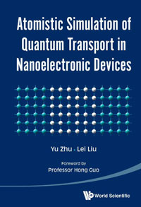
Atomistic Simulation of Quantum Transport in Nanoelectronic Devices:(With CD-ROM) |
|
| In this book, the authors conduct an experiment and adopt a "paradigm" approach. Instead of organizing materials by fields, they focus on the development of one particular software tool called NanoDsim, and provide relevant knowledge and techniques whenever needed. The black of box of NanoDsim is opened, and the complete procedure from theoretical derivation, to numerical implementation, all the way to device simulation is illustrated. The affilicated source code of NanoDsim also provides an open platform for new researchers. |
| Source: World Scientific |
