Crystalline fault lines provide pathway for solar cell current (w/video)
(Nanowerk News) A team of scientists studying solar cells made from cadmium telluride, a promising alternative to silicon, has discovered that microscopic "fault lines" within and between crystals of the material act as conductive pathways that ease the flow of electric current. This research—conducted at the University of Connecticut and the U.S. Department of Energy's Brookhaven National Laboratory, and described in the journal Nature Energy ("Charge transport in CdTe solar cells revealed by conductive tomographic atomic force microscopy"), may help explain how a common processing technique turns cadmium telluride into an excellent material for transforming sunlight into electricity, and suggests a strategy for engineering more efficient solar devices that surpass the performance of silicon.
"If you look at semiconductors like silicon, defects in the crystals are usually bad," said co-author Eric Stach, a physicist at Brookhaven Lab's Center for Functional Nanomaterials (CFN). As Stach explained, misplaced atoms or slight shifts in their alignment often act as traps for the particles that carry electric current—negatively charged electrons or the positively charged "holes" left behind when electrons are knocked loose by photons of sunlight, making them more mobile. The idea behind solar cells is to separate the positive and negative charges and run them through a circuit so the current can be used to power houses, satellites, or even cities. Defects interrupt this flow of charges and keep the solar cell from being as efficient as it could be.
But in the case of cadmium telluride, the scientists found that boundaries between individual crystals and "planar defects"—fault-like misalignments in the arrangement of atoms—create pathways for conductivity, not traps.
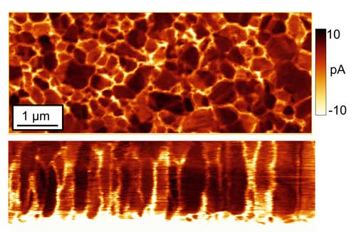
These CTAFM images show a cadmium telluride solar cell from the top (above) and side profile (bottom) with bright spots representing areas of higher electron conductivity. The images reveal that the conductive pathways coincide with crystal grain boundaries. (Image: University of Connecticut)
Members of Bryan Huey's group at the Institute of Materials Science at the University of Connecticut were the first to notice the surprising connection. In an effort to understand the effects of a chloride solution treatment that greatly enhances cadmium telluride's conductive properties, Justin Luria and Yasemin Kutes studied solar cells before and after treatment. But they did so in a unique way.
Several groups around the world had looked at the surfaces of such solar cells before, often with a tool known as a conducting atomic force microscope. The microscope has a fine probe many times sharper than the head of a pin that scans across the material's surface to track the topographic features—the hills and valleys of the surface structure—while simultaneously measuring location-specific conductivity. Scientists use this technique to explore how the surface features relate to solar cell performance at the nanoscale.
But no one had devised a way to make measurements beneath the surface, the most important part of the solar cell. This is where the UConn team made an important breakthrough. They used an approach developed and perfected by Kutes and Luria over the last two years to acquire hundreds of sequential images, each time intentionally removing a nanoscale layer of the material, so they could scan through the entire thickness of the sample. They then used these layer-by-layer images to build up a three-dimensional, high-resolution 'tomographic' map of the solar cell—somewhat like a computed tomography (CT) brain scan.
Assembling the layer-by-layer CTAFM scans into a side-profile video file reveals the relationship between conductivity and planar defects throughout the entire thickness of the cadmium telluride crystal, including how the defects appear to line up to form continuous pathways of conductivity. (Video: University of Connecticut)
"Everyone using these microscopes basically takes pictures of the 'ground,' and interprets what is beneath," Huey said. "It may look like there's a cave, or a rock shelf, or a building foundation down there. But we can only really know once we carefully dig, like archeologists, keeping track of exactly what we find every step of the way—though, of course, at a much, much smaller scale."
The resulting CT-AFM maps uniquely revealed current flowing most freely along the crystal boundaries and fault-like defects in the cadmium telluride solar cells. The samples that had been treated with the chloride solution had more defects overall, a higher density of these defects, and what appeared to be a high degree of connectivity among them, while the untreated samples had few defects, no evidence of connectivity, and much lower conductivity.
Huey's team suspected that the defects were so-called planar defects, usually caused by shifts in atomic alignments or stacking arrangements within the crystals. But the CTAFM system is not designed to reveal such atomic-scale structural details. To get that information, the UConn team turned to Stach, head of the electron microscopy group at the CFN, a DOE Office of Science User Facility.
"Having previously shared ideas with Eric, it was a natural extension of our discovery to work with his group," Huey said.
Said Stach, "This is the exact type of problem the CFN is set up to handle, providing expertise and equipment that university researchers may not have to help drive science from hypothesis to discovery."
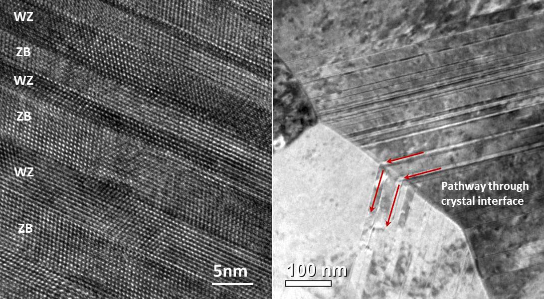
CFN staff physicist Lihua Zhang used a transmission electron microscope (TEM) and UConn's results as a guide to meticulously study how atomic scale features of chloride-treated cadmium telluride related to the conductivity maps. The TEM images revealed the atomic structure of the defects, confirming that they were due to specific changes in the stacking sequence of atoms in the material. The images also showed clearly that these planar defects connected different grains in the crystal, leading to high-conductivity pathways for the movement of electrons and holes.
"When we looked at the regions with good conductivity, the planar defects linked from one crystal grain to another, forming continuous pathways of conductance through the entire thickness of the material," said Zhang. "So the regions that had the best conductivity were the ones that had a high degree of connectivity among these defects."
These transmission electron microscopy images taken at Brookhaven's CFN reveals how the stacking pattern of individual atoms (bright spots) shifts. The images confirmed that the bright spots of high conductivity observed with CTAFM imaging at UConn occurred at the interfaces between two different atomic alignments (left) and that these "planar defects" were continuous between individual crystals, creating pathways of conductivity (right). The labels WZ and ZB refer to the two atomic stacking sequences "wurtzite" and "zinc blende," which are the two types of crystal structures cadmium telluride can form. (click on image to enlarge)
The authors say it's possible that the chloride treatment helps to create the connectivity, not just more defects, but that more research is needed to definitively determine the most significant effects of the chloride solution treatment.
In any case, Stach says that combining the CTAFM technique and electron microscopy, yields a "clear winner" in the search for more efficient, cost-competitive alternatives to silicon solar cells, which have nearly reached their limit for efficiency.
"There is already a billion-dollar-a-year industry making cadmium telluride solar cells, and lots of work exploring other alternatives to silicon. But all of these alternatives, because of their crystal structure, have a higher tendency to form defects," he said. "This work gives us a systematic method we can use to understand if the defects are good or bad in terms of conductivity. It can also be used to explore the effects of different processing methods or chemicals to control how defects form. In the case of cadmium telluride, we may want to find ways to make more of these defects, or look for other materials in which defects improve performance."