| Posted: Jun 27, 2017 |
New 'gold standard' for flexible electronics
(Nanowerk News) What if solar panels were both more efficient and more rugged? A new economical process makes optically transparent, flexible, and conductive gold films that could answer that question. The process deposits a single crystal gold film (Science, "Epitaxial lift-off of electrodeposited single crystal gold foils for flexible electronics").
|
|
The ability to grow single crystal gold is one of the vital scientific characteristics that allows device-grade electronics to be built.
|
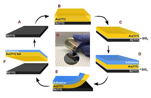 |
| A new recipe for making thin gold (Au) films for electronics starts with a silicon (Si) wafer (A), the standard starting surface for microelectronics. A thin layer of gold (B) is deposited onto the silicon by a process that results in an ordered gold layer. The gold layer contained pores due to the process. The silicon-gold layers are immersed in an acid bath, and a silicon oxide (SiOx) layer forms between the silicon-gold layers (C). An adhesive layer is applied on top of the gold foil (D), and another acid is used to remove the silicon oxide (E). The gold-adhesive foil is detached from the silicon (F), allowing the silicon to be reused. The resulting gold foil is very flexible (G) and conductive; it can be used in flexible electronics. (Image: Jay Switzer)
|
|
The new process can enable flexible electronic devices. Such devices include wearable solar cells, sensors, and flexible displays with superior properties.
|
|
Researchers developed a simple and inexpensive new process for making single crystalline, wafer-size, flexible, transparent, and conductive gold foils using a silicon wafer as a template.
|
|
The new process for making crystalline gold foil is valuable for flexible electronic devices such as wearable solar cells, sensors, and flexible displays. Gold was deposited from solution while applying an electric current (through a process called electrodeposition) onto an atomically ordered silicon wafer as a template, resulting in a gold film that was also crystalline (due to a process called epitaxial growth).
|
|
Other film fabrication methods, such as vapor deposition, result in polycrystalline gold films, which are not preferred due to their poor electronic properties and less efficient devices.
|
|
New in this research, scientists removed the ordered gold foil from the silicon wafer by forming a silicon oxide that could be etched away.
|
|
The silicon oxide formation was a two-step process. First, using the pores in the gold foil, water was able to reach the gold-silicon interface, providing oxygen to the surface. Second, the chemical reaction was catalyzed by exposure to light through a process called photoelectrochemical oxidation.
|
|
The gold foil was used as a template for the fabrication of three types of flexible electronic devices:
|
|
A diode formed by the deposition of an inorganic semiconductor cuprous oxide
An organic light-emitting diode (OLED) by spin coating of the organic light emitter tris(bipyridyl)ruthenium(II)
Zinc oxide nanowires that can be used as a wide band gap semiconductor and in piezoelectric applications.
|
|
All three types of devices showed excellent device characteristics. For the materials tested for mechanical properties, the gold films and zinc oxide nanowires, the quality did not degrade after several hundred bending cycles, demonstrating the viability of the gold films in flexible electronics applications. The gold itself can also be used as a device, such as a wearable sensor.
|