| May 08, 2024 |
Scientists observe and analyze a phenomenon that combines optical-electrical-mechanical properties in a 2D atomic layer
(Nanowerk News) The results of observation and analysis of a phenomenon that combines optical, electrical, and mechanical properties in a two-dimensional atomic layer were revealed by a joint Korean-American research team and published in Nano Letters ("Optically Triggered Emergent Mesostructures in Monolayer WS2").
|
|
The Gwangju Institute of Science and Technology (GIST) announced that a team of researchers led by Senior Researcher Sang-Youp Yim of the Advanced Photonics Research Institute and collaborators from the University of Pennsylvania in the United States have identified polarons (a quasiparticle concept introduced to understand the interaction between charge carriers and atoms in solid materials) as the cause of the phenomenon that causes thin films to swell and locally change semiconductor doping properties when light is shone on a two-dimensional atomic layer.
|
 |
| Expansion of the WS2 atomic layer depending on the intensity of light. As a result of observing the change in surface height while injecting a red laser beam into the WS2 atomic layer, a reversible expansion phenomenon was observed depending on the intensity of light. Similar results were obtained with a blue laser beam that can be absorbed by the WS2" atomic layer, but there was no change with a near-infrared laser beam without absorption. (©ACS Nano)
|
|
Two-dimensional semiconductor materials, which utilize two-dimensional nanomaterials instead of silicon, are promising future materials because of their unique electrical, optical, chemical, and mechanical properties, but the phenomenon of how these properties are combined is not yet clearly understood.
|
|
One of these phenomena is photocompression (or photodilation), which is the change in size or shape of a sample when light is shone on it without applying heat. If photocompression or photodilation occurs in a two-dimensional layer of atoms, it is possible to develop nanosystems that can control mechanical motion at the nanometer scale.
|
|
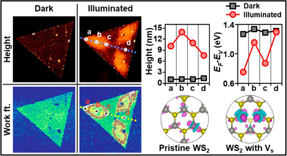
As a result of observing the change in surface height with an atomic force microscope by applying a red laser beam to the tungsten disulfide (WS2") atomic layer, it was observed that the area with few defects began to swell first, resulting in a symmetrical expansion pattern. It was confirmed that this is a reversible phenomenon in which it expands significantly as the intensity of light increases, and returns to its original state when no light is applied. A similar phenomenon was observed when using a blue laser instead of a red laser.
|
|
However, the near-infrared laser, which is not absorbed by the WS2" atomic layer, showed no change even when fired at very high intensity. It was confirmed that charge carriers and defects excited by absorbed light play an important role.
|
|
The research team observed with a Kelvin microscope that the semiconductor doping characteristics change in a local area depending on the intensity of light and a local p-n junction occurs. As a result, it was found that the electron-polaron state bound to the defect is the cause of lattice expansion and local change in semiconductor doping characteristics.
|
|
The research team discovered that when light shines on the atomic layer of WS2", a type of transition metal dichalcogenide two-dimensional semiconductor thin film, the thin film swells into a patterned shape and the semiconductor doping characteristics change in a local region, forming a local p-n junction. This phenomenon was observed, and it was revealed that electron-polarons were the cause.
|
|
The observation and analysis of a phenomenon that combines optical, electrical, and mechanical properties in a two-dimensional atomic layer is the world's first research result reported by the research team.
|
|
Senior Researcher Sang-Youp Yim said, "This research will serve as a cornerstone of attempts to observe similar phenomena in various 2D semiconductor materials and to control the type/density of defects. It is expected that it will be possible to develop optical nano actuators that are ultra-small and operate at low power in the future."
|

