Understanding Thin Films: Key to Advanced Electronics, Optics, & Energy
Definition: Thin films are critical layers of material, from a few nanometers to several micrometers thick, deployed across technology, electronics, and energy sectors. Their importance lies in their ability to alter the physical properties of surfaces in ways bulk materials cannot, primarily due to their reduced dimensions.
Core Materials and Devices
Thin films can be made from a variety of materials, including metals (e.g., gold, silver), oxides (e.g., silicon dioxide, titanium dioxide), and semiconductors (e.g., silicon, gallium arsenide). These materials are foundational in creating devices such as transistors, light-emitting diodes (LEDs), and photovoltaic cells. The choice of material directly influences the film's electrical, optical, and mechanical properties, thereby determining the functionality of the device.
Nanotechnology and Thin Films
At the nanoscale, thin films exhibit unique properties that are not present in their bulk form. This is due to the quantum effects that dominate at these scales, affecting electron behavior and material characteristics. The ability to control film thickness with nanometer precision allows for the tuning of these properties, enabling advancements in nanoelectronics, optoelectronics, and energy devices. This precision underscores the significance of thin films in the field of nanotechnology.
Deposition Techniques
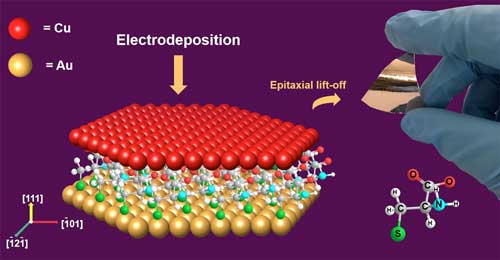
The deposition of thin films employs methods such as physical vapor deposition (PVD) and chemical vapor deposition (CVD). Each technique has its benefits, with PVD being preferred for its physical process of transferring materials to the substrate, while CVD is favored for its chemical reaction-based process, allowing for finer control over the film's chemical composition. Advanced deposition techniques, including atomic layer deposition (ALD), further refine these processes for nanoscale precision.
Impact on Industry and Research
The applications of thin films are extensive and varied. In the electronics industry, they are integral to the manufacturing of semiconductors and passive components. Optically, they are used to create reflective and anti-reflective coatings, as well as filters. Energy technologies benefit from thin films in the efficiency improvements of photovoltaic cells and the capacity enhancement of batteries. Moreover, the field of protective coatings utilizes thin films to enhance material durability against environmental degradation.
Challenges in Thin Film Technology
Despite their widespread application, the production of thin films faces challenges, including achieving uniform thickness across large areas, controlling the stoichiometry and crystallinity of the films, and ensuring strong adhesion to various substrates. Ongoing research is dedicated to overcoming these obstacles, with a focus on developing new materials, enhancing deposition techniques, and understanding the fundamental properties of thin films at the nanoscale.
Future Directions and Sustainability
Innovations in thin film technology continue to push the boundaries of what is possible in nanotechnology and materials science. The development of new materials and deposition methods is paving the way for the next generation of electronic, optical, and energy devices. Additionally, thin films play a crucial role in sustainable technology development, contributing to the production of more efficient solar cells and energy storage systems, which are vital for the transition to green energy.
Further Reading
Materials Today: Proceedings, Review of thin film deposition and techniques
Applied Optics, Review of the fundamentals of thin-film growth
Materials Research Express, A review on thin films, conducting polymers as sensor devices
