| Posted: May 12, 2017 | |
What ultimately limits the scaling of graphene nanogap electrodes(Nanowerk News) The ability to create nanometer-sized gaps in sp2-bonded carbon materials offers a means of contacting nanoscale objects, for example, nanocrystals and single molecules, that cannot be achieved with conventional metallic electrodes. |
|
| Scientists have found that the intense electric fields generated by applying a bias voltage across a nanometer-size graphene gap result in the spontaneous rearrangement of atoms and bonds that lead to reversible switching of the resistance. | |
| In new work, researchers at the University of Oxford investigate the scaling limits imposed by this switching behavior in the context of phase change memory (PCM) devices. However, their findings carry equal significance for all applications based on graphene nanogaps, including single-molecule electronics and graphene-based genome sequencing. | |
| The paper has been published in Nano Letters ("Scaling Limits of Graphene Nanoelectrodes"). | |
| In this paper, the team finds that it is the intrinsic switching behavior of the graphene electrodes, rather than the properties of the phase change material, that ultimately limits the device scaling and therefore its performance. | |
 |
|
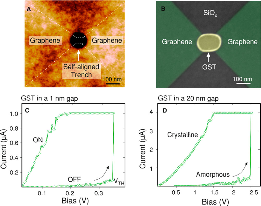
| Self-alignment approach and phase change memory device. (A) AFM image showing a trench of size 148 nm (largest lateral dimension) in PMMA. This trench is formed in situ from local degradation of PMMA due to Joule heating during the electroburning process. Dotted line outlines the graphene ribbon underneath PMMA. (B) Colored SEM image of a self-aligned PCM device showing the phase change material (GST) in the nanogap. The trench in the PMMA ensures that the GST is self-aligned to the gap in the graphene electrodes, thus eliminating the need for sub-10 nm alignment. (C) Current-voltage trace of a GST nanogap device; GST is aligned to make contact to graphene in a 1 nm nanogap. The device switches from a high resistive state to a low resistive state in ambient conditions at a switching voltage of 370 mV and current 100 nA. (D) Current-voltage characteristics of a GST device with a gap size of ∼20 nm. GST switches from a highly resistive amorphous state to a less resistive crystalline state at a bias of 2.5 V and current 500 nA. The ratio of resistance between these states averages to ~∼1000. (© ACS) (click on image to enlarge) | |
| The authors write that "our observations indicate resistance switching in graphene nanogaps, which we attribute to the controlled formation and breakdown of carbon filaments. Analyzing the switching behavior, we find that the formation of carbon filaments is electric field dependent and only occurs in sub-5 nm gaps." | |
| These experiments demonstrate for the first time, reversible resistance switching in graphene nanogaps in ambient conditions. For PCM devices with electrode separations less than 5 nm, the scientists find the resistance switching to be fully dominated by the formation of carbon filaments. | |
| They point out that "whereas the actual mechanisms that we propose (carbon filamentation) need further unambiguous proof, nonetheless our results point toward a key scaling limit to using such electrodes." | |
| Although the potential formation of graphene filaments poses challenges to the development of graphene-based nanoelectrodes, it also offers exciting opportunities to study charge transport in atomic carbon chains. | |
| The authors conclude: "If these structures could be controllably formed between graphene nanoelectrodes, they could serve as a test bed for the observation of a plethora of transport phenomena predicted in atomic chains and could further also be extended for various applications such as all carbon-based transistors." |
 By
Michael
Berger
– Michael is author of three books by the Royal Society of Chemistry:
Nano-Society: Pushing the Boundaries of Technology,
Nanotechnology: The Future is Tiny, and
Nanoengineering: The Skills and Tools Making Technology Invisible
Copyright ©
Nanowerk LLC
By
Michael
Berger
– Michael is author of three books by the Royal Society of Chemistry:
Nano-Society: Pushing the Boundaries of Technology,
Nanotechnology: The Future is Tiny, and
Nanoengineering: The Skills and Tools Making Technology Invisible
Copyright ©
Nanowerk LLC
|
|
|
Subscribe to a free copy of one of our daily Nanowerk Newsletter Email Digests with a compilation of all of the day's news. |