| Posted: Jun 03, 2017 | |
Overcoming hysteresis in carbon nanotube field effect transistors(Nanowerk News) Researchers have developed a facile approach to overcoming hysteresis in carbon nanotube field-effect transistors (CNFETs) to <0.5% of the gate-source voltage (VGS) sweep range: rather than to eliminate traps, they aim to reduce the effect that traps have on the carbon nanotubes (CNTs). |
|
| These findings have been reported in ACS Nano ("Hysteresis-Free Carbon Nanotube Field-Effect Transistors"). | |
 |
|
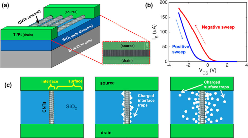
| Sources of hysteresis in CNFETs. (a) A typical CNFET structure with a highly doped silicon substrate as a gate, thermally grown SiO2 as the gate dielectric, and CNTs as the channel material between the source and drain contacts. Inset shows SEM image of CNTs across source and drain. (b) IS-VGS curve of a CNFET such as (a). Large hysteresis is observed in this device structure between the positive sweep and the negative sweep. (c) Illustration of the progression of the charge trapping process at the interface traps and surface traps which are the dominant sources of hysteresis. (© ACS) (click on image to enlarge) | |
| Large hysteresis remains a major obstacle facing energy-efficient CNFET digital logic as hysteresis degrades system-level performance – e.g., by reducing noise margin and increasing delay variations. | |
| As the authors point out, due to a CNT’s one-dimensional geometry, the physics behind hysteresis is different from a conventional two-dimensional semiconductor device. | |
| Using the physics-based model from the team's previous work (ACS Nano, "Hysteresis in Carbon Nanotube Transistors: Measurement and Analysis of Trap Density, Energy Level, and Spatial Distribution"), they illustrate the interaction between the metal gate, the traps, and the carbon nanotube. | |
 |
|
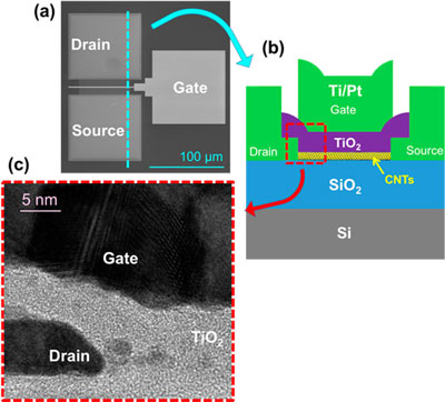
| CNFET structure. (a) An SEM image of a top view of a fabricated top-gated CNFET. (b) A cross-sectional schematic. (c) A TEM image showing the 5 nm deposited TiO2. The amorphous structure of TiO2, along with the fabrication process, ensures minimal leakage current through the gate electrode. (© ACS) | |
| In their work, the authors show that hysteresis is naturally overcome by scaling the gate dielectric thickness in CNFETs, even without optimizing the interfaces to minimize traps. | |
| However, they write that despite reducing hysteresis, large subthreshold swing remains a challenge and is attributed to single-CNT threshold voltage (VT) variations. | |
| "The VT variations cannot be entirely attributed variations in CNT diameter, but rather additional non-ideal aspects of device processing contribute a non-negligible portion," the scientists conclude. "Therefore, the next major challenge is to control single-CNT VT to achieve steep subthreshold swing for multiple-CNT CNFETs, which will require further work to improve the interface qualities. |
 By
Michael
Berger
– Michael is author of three books by the Royal Society of Chemistry:
Nano-Society: Pushing the Boundaries of Technology,
Nanotechnology: The Future is Tiny, and
Nanoengineering: The Skills and Tools Making Technology Invisible
Copyright ©
Nanowerk LLC
By
Michael
Berger
– Michael is author of three books by the Royal Society of Chemistry:
Nano-Society: Pushing the Boundaries of Technology,
Nanotechnology: The Future is Tiny, and
Nanoengineering: The Skills and Tools Making Technology Invisible
Copyright ©
Nanowerk LLC
|
|
|
Subscribe to a free copy of one of our daily Nanowerk Newsletter Email Digests with a compilation of all of the day's news. |