| Posted: Aug 12, 2017 | |
Achieving sub-30nm resolution with self-collapse lithography(Nanowerk News) Several molecular patterning strategies have been developed as economical and accessible alternatives to conventional nanofabrication methods, including soft lithographic microcontact printing (µCP), replica molding, nanoimprint lithography, polymer pen lithography, nanotransfer printing, decal transfer printing, and nanoskiving. |
|
| The most widely utilized of these methods, µCP, achieves microand nanoscale patterning of molecular 'inks' (e.g., alkanethiols or biomolecules) via stamps replica-molded from masters prepared by conventional photolithography. | |
| However, the quality of the final patterns produced via µCP is limited by a variety of factors, including diffusion of molecular inks and/or the deformation of stamp features. | |
| In new work, researchers demonstrate control of self-collapse behavior of polydimethylsiloxane (PDMS) stamps precisely at the nanoscale when integrated with chemical lift-off lithography (CLL) to establish a new nanolithography method: self-collapse lithography (SCL). | |
| As the team from UCLA reports in Nano Letters ("Self-Collapse Lithography"), using SCL, they achieve sub-30 nm features by tailoring the dimensions of the stamp features, as well as the stiffness of the PDMS. | |
 |
|
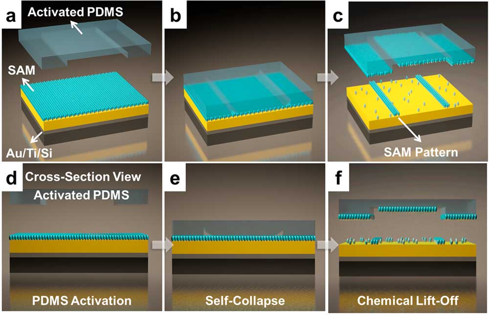
| Schematic illustration of self-collapse lithography (SCL). (a,d) Hydroxyl-terminated alkanethiols form a self-assembled monolayer (SAM) on the surface of a Au/Ti-coated Si substrate. A polydimethylsiloxane (PDMS) stamp is activated by oxygen plasma treatment. (b,e) The activated stamp is brought into conformal contact with the SAM-coated Au surface without externally applied forces. (c,f) The chemical lift-off process removes the SAM from regions of the functionalized surface in direct contact with the stamp, thereby producing a pattern from molecules remaining in noncontacted regions. (© ACS) (click on image to enlarge) | |
| SCL represents a facile and robust nanolithography technique to achieve sub-30 nm resolution by exploiting the elasticity of PDMS structures and natural stamp-substrate adhesion forces. A wide range of shapes and feature sizes can be patterned by strategically designing stamp feature dimensions (e.g., height/width) and/or Young’s modulus. | |
| Importantly, this soft-lithographic approach can be used as a complement or alternative to slow and expensive direct-writing processes (e.g., electron-beam lithography). | |
| The SCL technique provides new insight into how a previously undesirable characteristic of soft lithography can be exploited, via CLL, to yield nanoscale patterns. | |
| Finite element model simulations suggest a straightforward mechanism for the self-collapse process through the competition between restoring and adhesion stresses along the gap edge produced between the protruding and collapsed stamp features. | |
| "Results from these simulations correlate well with experimental data and elucidate design rules for using controlled self-collapse to generate complex patterns at the nanoscale that can be applied broadly to applications in nanoelectronics, biosensing, energy storage, and catalysis," the authors conclude their report. |
 By
Michael
Berger
– Michael is author of three books by the Royal Society of Chemistry:
Nano-Society: Pushing the Boundaries of Technology,
Nanotechnology: The Future is Tiny, and
Nanoengineering: The Skills and Tools Making Technology Invisible
Copyright ©
Nanowerk LLC
By
Michael
Berger
– Michael is author of three books by the Royal Society of Chemistry:
Nano-Society: Pushing the Boundaries of Technology,
Nanotechnology: The Future is Tiny, and
Nanoengineering: The Skills and Tools Making Technology Invisible
Copyright ©
Nanowerk LLC
|
|
|
Subscribe to a free copy of one of our daily Nanowerk Newsletter Email Digests with a compilation of all of the day's news. |