| Posted: September 8, 2009 |
How to make cheap nanostructures of a luminescent conjugated polymer with micron-sized tools |
|
(Nanowerk News) Researchers from the London Centre for Nanotechnology (LCN) and University College London (UCL) have fabricated sub-30 nm luminescent features of an organic semiconductor via spatially selective conversion and patterning of its precursor by using a heatable, micron-size scanning probe (see figure below). The results will soon be reported in the journal Nature Nanotechnology.
|
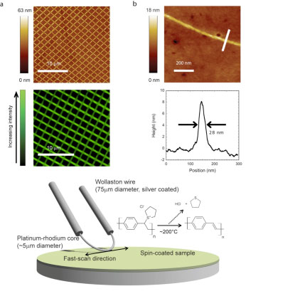 |
| A schematic of the Wollaston wire probe and the lithographic process (bottom). a Regular patterns drawn over large areas using scanning thermochemical lithography. The top image is an atomic force micrograph, whilst the bottom image is from a confocal microscope. b Atomic force microscope image of a high resolution lithographic line (top) and its cross-section (bottom).
|
|
The future development of electronics and photonics relies on a range of sophisticated lithographyic techniques for the patterning of semiconducting, dielectric, and metallic materials. Researchers at the London Centre of Nanotechnology (LCN), the Department of Physics and Astronomy, and the Eastman Dental Institute at UCL, have now developed a thermochemical patterning technique for materials known as organic semiconductors.
|
|
These materials can be used in light-emitting diodes (LEDs), solar cells, lasers and transistors, and their potential is in low processing costs and the ability to build devices on flexible substrates. However, applications of these materials in nanoelectronics and nanophotonics are limited by the range of patterning techniques available. Many of the approaches to nanolithography that are used to pattern inorganic materials, such as e-beams or Focused Ion Beams (FIBs), are too harsh for organic semiconductors, that can be damaged by the high energy of the patterning beams, or by the chemicals needed for the processing.
|
|
So, instead of using standard optical or other “conventional” high-resolution lithographies, the UCL researchers used a small heat source for the patterning. This heat source, known as a modified Wollaston wire, can be mounted on an atomic force microscope and scanned across surfaces to chemically convert all areas it comes into contact with. This technique has allowed the UCL researchers to achieve patterned resolutions below 28 nm and write speeds of 100 µm/s in the widely used organic semiconductor, PPV. The result is particularly surprising given the large diameter of the heat source (5 µm) compared to the resolutions achieved, and since it is likely that resolution could be further improved with the use of nanoscale heat sources, as already reported by other groups.
|
|
There has already been some commercial interest in using atomic force microscopes to pattern surfaces, as for example by IBM in their ‘millipede’ project, that was aimed at data-storage applications, but such a thermochemical approach opens up new possibilities. In particular, this work shows that thermochemical lithography offers a versatile, simple and reliable nanopatterning technique. For example, thermo-crosslinkable additives could easily be added to a variety of other solution-processible semiconductors. The technique should also be generally applicable to other classes of materials. A large number of optical materials, including many commercial cross-linker additives and photoresists, rely in fact on chemical mechanisms that can also be thermally activated.
|
|
The group, led by Franco Cacialli, has previously used scanning near-field optical lithography (SNOL) for nanopatterning of PPV structures from the same precursor polymer, poly(p-xylene tetrahydrothiophenium chloride) (PXT). This work included the fabrication of quasi-periodic two-dimensional structures with potential for photonic applications. However, the thermochemical technique now developed (Scanning Thermal lithography, or SThL) enables one to bypass the UV insolubilisation step, and the complications and additional costs imposed by the needs for lasers, optics, and sophisticated optical fibre probes.
|
|
References
|
|
[1] n.a.
|
|
[2] Szoszkiewicz, R. et al., High-Speed, Sub-15 nm Feature Size Thermochemical Nanolithography. Nano Lett. 7, 1064-1069 (2007).
|
|
[3] Riehn, R., Charas, A., Morgado, J., & Cacialli, F., Near-field optical lithography of a conjugated polymer. Appl. Phys. Lett. 82, 526-528 (2003).
|
|
[4] Riehn, R. & Cacialli, F., A two-dimensional photonic structure made from a conjugated, fluorescent polymer. J. Opt. A: Pure Appl. Opt. 7, S207-S212 (2005).
|
|
About the London Centre for Nanotechnology
|
|
The London Centre for Nanotechnology is a UK-based, multidisciplinary research centre forming the bridge between the physical and biomedical sciences. It was conceived from the outset with a management structure allowing for a clear focus on scientific excellence, exploitation and commercialisation. It brings together two world leaders in nanotechnology, namely University College London and Imperial College London, in a unique operating model that accesses the combined skills of multiple departments, including medicine, chemistry, physics, electrical and electronic engineering, biochemical engineering, materials and earth sciences, and two leading technology transfer offices.
|