| Posted: February 17, 2010 |
Semiconductor processing: Stress management |
|
(Nanowerk News) Specialized sensors to measure the amount of mechanical stress caused by the process to thin semiconductor wafers—used to pack ever-increasing amounts of processing power into ever-decreasing spaces—have been designed, fabricated and calibrated by an international research team involving A*STAR researchers.
|
|
“The demand for miniaturization and the integration of many functions into a single product has led to the development of chip-stacking technology,” says team member Xiaowu Zhang from the A*STAR Institute of Microelectronics. However, fabrication technology has advanced to the point where the density of devices on the surface of a semiconductor wafer is approaching the limits imposed by physics. Reducing the substrate thickness allows for further space savings, but the thinning induces a residual stress in the wafers that makes them susceptible to damage.
|
|
Zhang and his co-workers in collaboration with scientists from the Georgia Institute of Technology, USA, and Infineon Technologies, Germany, therefore studied the stresses that silicon substrates must endure because of the thinning process ("Application of piezoresistive stress sensors in ultra thin device handling and characterization "). First, the team needed to develop in situ sensors. As luck would have it, silicon has very strong piezoresistive properties; that is, an applied force changes its electrical resistance.
|
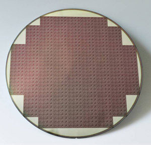 |
| Fig. 1: A photograph of an 8-inch (20 cm) silicon wafer fabricated with a grid of stress sensors to measure changes in residual stress during mechanical back grinding. (© 2010 Xiaowu Zhang)
|
|
They defined stress-sensitive resistors, 80–100 micrometers in width and 350–420 micrometers in length, at various places on a silicon substrate (Fig. 1) using chemical etching and by introducing atomic impurities. By bending a sensor strip to induce a known force, they precisely calibrated each device. By grinding the sample with microscopic particles, they reduced the sample thickness before polishing to remove any remaining cracks. Experiments by the team then showed that the residual stress increased by a factor of seven as the wafer, initially 400 micrometers thick, was reduced to a width of just 100 micrometers. This is believed to be a result of warping, which is more prevalent in thinner layers.
|
|
Handling wafers that are so fragile is also a practical difficulty, but Zhang and his co-workers have devised a solution to this too. They attached the thin sample to a thicker silicon substrate using a layer of adhesive. This easy-to-handle support was perforated with holes to enable the adhesive to be dissolved in solution whenever the ultra-thin layer was to be released.
|
|
These results and the ability to handle very delicate wafers reduce the chance of damage during processing. This in turn could lead to more advanced devices: memory stacking in mobile phones and sensors in digital single-lens reflex (SLR) cameras are just two examples given by Zhang.
|