| Posted: November 18, 2008 |
Photonics Advanced Research Center at Osaka University and SPIE sign cooperation agreement |
|
(Nanowerk News) The Photonics Advanced Research Center (PARC) at Osaka University and SPIE have signed an agreement to cooperate more closely in fostering information exchange and other activities to help advance photonics research.
|
|
The Memorandum of Understanding was signed by Satoshi Kawata, Director of PARC, and Kevin Harding, SPIE President, in Osaka earlier this month.
|
|
"SPIE is very pleased to have the opportunity to work more closely with the Photonics Advanced Research Center at Osaka University in meeting our shared goals of furthering interdisciplinary research in optics, photonics, and nanotechnology, and of translating academic knowledge into technological innovation," Harding said. "Osaka University is among the world's most highly respected research centers, and SPIE is very enthusiastic about the possibilities for increased sharing of information and for expanded educational partnerships that are enabled by this collaboration."
|
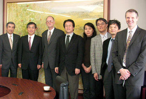 |
| SPIE President Kevin Harding visited Osaka University this month. Present were, from left, Prof. Kiichiro Tsuji, Trustee/Vice President, Osaka University; Prof. Shojiro Nishio, Trustee/Vice President, Osaka University; Harding; Prof. Satoshi Kawata, Director of the Photonics Advanced Research Center (PARC) at Osaka University; Dr. Masako Yamada, GE Global Research; Prof. Eiichi Tamiya, Vice Director of PARC; Dr. Hiroshi Iwasaki, Program Manager, PARC, and Professor Emeritus, Osaka University; and Dr. Andrew Brown, SPIE Senior Director of Global Business Development.
|
|
Under the agreement, PARC and SPIE will exchange information about activities such as technical conferences, educational and professional development programs, publications, scholarships, and grants, and will communicate about trends in the field and other issues. The agreement will enable increased participation and visibility of members, faculty, and students in networking opportunities, educational collaborations, Visiting Lecturer exchanges, and other programs.
|
|
Harding and Andrew Brown, SPIE Senior Director of Global Business Development, met with PARC leadership in conjunction with a Photonics Day informational event for students and young researchers. PARC faculty outlined the center's goals, the advantages of university-industry cooperation, and the center's research. Harding gave a talk on "The Art of Invention: Optics and the Recording of Knowledge."
|
|
PARC's focus is on research enabling technology innovation in biotechnology, communications, security, environmental health, energy conservation, and other areas.
|