| Posted: January 28, 2009 |
Conducting domain walls could be the ultimate feature for future nanoelectronics |
|
(Nanowerk News) The logic and memory functions of future electronic devices could shrink dramatically – to one or two nanometers instead of the many tens of nanometers that characterize today’s most advanced elements - if a way can be found to control domain walls, the ultrathin transition zones that separate regions of a material having different magnetic, electric, or other properties.
|
|
In a material called bismuth ferrite, an unusual compound of bismuth, iron, and oxygen (BiFe03), scientists at the Department of Energy’s Lawrence Berkeley National Laboratory and the University of California at Berkeley have discovered a property of domain walls never seen before ("Conduction at domain walls in oxide multiferroics"). Although bismuth ferrite is an insulator, the researchers found that between domains having different electrical polarization, the domain walls themselves – just two nanometers wide – conduct electricity at room temperature.
|
|
“A domain wall is virtually a two-dimensional sheet through the material,” says Ramamoorthy Ramesh of Berkeley Lab’s Materials Sciences Division (MSD), a professor in the Department of Materials Science and Engineering and the Department of Physics at UC Berkeley. “Because they are so small and can be moved, domain walls have great promise for future electronics.”
|
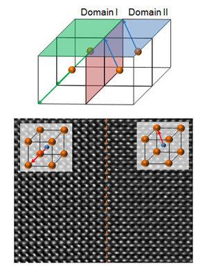 |
| Bismuth ferrite is an insulator, but different domains may have different electrical polarizations. The position of the central iron atom and the displacement of the bismuth atoms in each cubic cell determine the polarization of the domain. In this transmission electron image, structural changes appear near and inside the wall. As a consequence, the domain walls themselves (dotted line), which are just two nanometers wide, can conduct electricity at room temperature.
|
|
Ramesh heads MSD’s Quantum Materials program for the study of complex materials, which is supported by the Office of Basic Energy Sciences (BES) within the Department of Energy’s Office of Science. Unlike familiar metals or semiconductors, the basic electrical and magnetic properties of complex materials are extremely sensitive to their environment, says Ramesh. “Materials called multiferroics are an example of this kind of material, and bismuth ferrite is a prototypical multiferroic.”
|
|
The promise of multiferroics
|
|
Multiferroics may be an unfamiliar term, but is not likely to remain so for long. It describes materials that simultaneously exhibit two or more ferroic properties – ferromagnetism, ferroelectricity, or ferroelasticity. Bismuth ferrite, for example, is antiferromagnetic and ferroelectric as well. (Ferrum is Latin for iron; magnetism in iron was the first ferroic property ever observed, in ancient times, but the term ferroics now extends to include compounds and properties having nothing to do with iron.)
|
|
Ferromagnetism is the most familiar kind of magnetism, characterized by fields oriented by north and south poles. Ferroelectricity refers to materials which can be electrically polarized, having a preferred orientation of positive-negative electric charge. In ferroelastic materials – “shape-memory” alloys, for example – stress can cause a spontaneous change in orientation or crystal structure that can flip back again. A multiferroic material may have regions, separated by domain walls, where one or more of these different properties are differently oriented.
|
|
“One reason we are looking at oxides like bismuth ferrite is because we can control one property by changing others,” says Ramesh. “These materials have a lot of personality.”
|
|
Jan Seidel of the UC Department of Physics came upon the unique domain-wall properties of bismuth ferrite as he was performing scanning-probe measurements on thin films of the material created by Lane Martin of MSD; both are members of the Quantum Materials program.
|
|
“To make the films we hit targets of ceramic oxides containing bismuth and iron with a laser pulse and convert the solid to a plasma plume that is deposited on the substrate,” Martin explains. “We choose the substrate structure and control the temperature and atmosphere to get the right mix and the right phase.”
|
|
For the present work Martin grew films of bismuth ferrite between 50 and 200 nanometers thick on substrates of strontium titanium oxide (SrTiO3), a crystal whose similar lattice parameters and structure encouraged the growth of high-quality bismuth ferrite films. (A thin layer of a different compound, strontium ruthenium oxide, SrRuO3, was first laid down between the substrate and the bismuth ferrite to serve as an electrode.)
|
|
Like many other multiferroic oxides, bismuth ferrite has the crystal structure of perovskite, in which planes of oxygen atoms and heavy atoms (like bismuth) alternate with planes of oxygen atoms and lighter atoms (like iron). An iron atom is at the center of the basic bismuth ferrite cubic cell, and its position – whether slightly off center in one direction or another – plus the positions of affected bismuth atoms, gives rise to local polarization.
|
|
The bismuth ferrite films contained ferroelectric domains between 5 and 10 micrometers (millionths of a meter) in dimension, and, says Seidel, “we can map and even change the domain structure by using different scanning-probe mechanisms.”
|
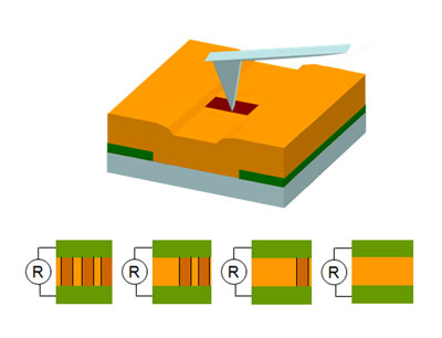 |
| Scanning probe tips can be used to control the number and arrangement of conducting domain walls in bismuth ferrite (gold) between electrodes (green), thus creating useful devices on the nanoscale. For example, current can be incrementally controlled by creating or erasing domain walls, as at bottom.
|
|
Bismuth ferrite is an insulator, but each domain has a distinct polarization or orientation of charge, which Seidel mapped using a piezoresponse force microscope (PFM): as the PFM probe moves across a sample, an alternating electric field in the tip gives rise to a detectable mechanical response in the sample, according to its polarization. The same PFM setup can control the nature of the local polarization of the film by applying a large enough voltage to switch it.
|
|
To map out the topographic features of the film surface, the scanning probe was used in atomic force microscopy (AFM) mode. In AFM the probe effectively “feels” its way across the surface, like a stylus in a record player feeling the grooves in a record. Moreover, by setting a voltage that is too slight to affect the polarization of the domains, the researchers can probe the electronic properties of the films.
|
|
In this mode (conducting AFM), Seidel measured the local conductivity of the sample across the domains and across domain walls. The domains were indeed nonconducting – since bismuth ferrite is an insulator – but surprisingly, certain domain walls exhibited electrical conductivity. Their conductivity depended on the angular difference in the direction of the polarization on either side of the domain wall.
|
|
To understand this unexpected conductivity, the researchers used transmission electron microscopy (TEM) at Berkeley Lab’s National Center for Electron Microscopy, a national user facility supported by BES, to inspect how the atoms were differently arranged, in the domains and near the domain walls. Bismuth ferrite’s domain walls are oriented along two distinct crystallographic planes; they can separate domains with either 109-degree, 71-degree, or 180-degree differences in the direction of polarization. By comparing the atomic structure of a nonconducting 71-degree domain wall to the atomic structure of a conducting 109-degree domain wall, the researchers found a clear difference in local structure: it promised to hold the key to understanding the origin of the effect.
|
|
How an insulating material’s domain walls can conduct electricity
|
|
“We worked with theorists to help us model the behavior we had observed and to understand the mechanism of the conduction,” says Ramesh. “What emerged was a clear picture of the changes in the structure of the unit cells of the bismuth ferrite near the domain walls.” These structural changes are directly connected to a local change in the electronic properties of the material at the center of the domain wall.
|
|
“What happens is that as the positions of the central iron atoms change crossing the domain wall, the polarization increases perpendicular to the domain wall – but at the same time goes to zero parallel to the wall, before increasing again,” says Martin. “This causes any free electrons in the vicinity to accumulate at the wall, where they can move along the wall itself.”
|
|
The researchers’ calculations also showed that the band gap of bismuth ferrite – a critical property for determining the electronic properties of materials used in electronic devices – decreased markedly in the center of the 109-degree and 180-degree domain walls, consistent with the increase in conductivity there. But in nonconducting 71-degree domain walls, the band gap decreased much less.
|
|
What strikes Seidel about these results “is the fundamental science. We have found a basic property of ferroelectric materials, and of ferroelectricity itself, that was not known before. Ferroelectrics have been studied for over half a century, but this is the first observation of this type of conduction.”
|
|
Martin is enthusiastic about the potential applications of their discovery. “Domain walls may be the ultimate nanoscale feature,” he says. “They’re intrinsic to the material – they want to be there. And they’re only two nanometers wide! It’s like shoving a graphene sheet” – a single layer of carbon atoms with remarkable conductive properties – “right down into a tough, insulating ceramic.”
|
|
For Ramesh, the discovery, in an oxide, of domain walls that conduct electricity like a metal is a step along “the path to the Holy Grail of oxide materials, the challenge of creating and controlling metal-insulator transitions at interfaces in a material. It’s why DOE is so interested in this kind of research.”
|