| Nov 28, 2012 |
Improving nanofabrication with nanodiamond tips
|
|
(Nanowerk News) One of the most promising innovations of nanotechnology has been the ability to perform rapid nanofabrication using nanometer-scale tips. Heating such tips can dramatically increase fabrication speeds, but high speed and high temperature have been known to blunt their atomically sharp points.
|
|
Now, research conducted by a team that included the University of Pennsylvania’s Robert Carpick and Tevis Jacobs has created a new type of nano-tip for thermal processing, which is made entirely made out of diamond.
|
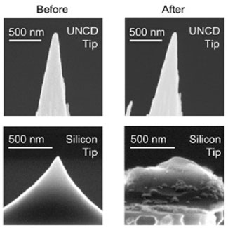 |
| Images of the researchers' diamond tips compared to traditional silicon tips, before and after scanning for 1.2 meters.
|
|
Carpick is a professor and chair of the Department of Mechanical Engineering and Applied Mechanics in the School of Engineering and Applied Science; Tevis is a doctoral student in Carpick’s lab. The research team was led by William King of the University of Illinois’ Department of Mechanical Science and Engineering and involved his group members Hoe-Joon Kim, Suhas Somnath and Jonathan Felts. Researchers from Advanced Diamond Technologies Inc., Mike Moldovan and John Carlisle, also contributed to the study.
|
|
Their work was published in the journal Nanotechnology ("Ultrananocrystalline diamond tip integrated onto a heated atomic force microscope cantilever").
|
|
For more than 20 years, researchers have been imaging nanoscale objects with atomic force microscopes, which use nanometer-scale tips to feel the push and pull of individual atomic forces. Researchers have also been interested in using these tips to etch surfaces or deposit materials in nano-manufacturing processes, but one of the key challenges has been the reliability of the tips, especially with performing nano-writing on hard, semiconductor surfaces.
|
|
Using a process known as reactive ion etching, the researchers were able to create a new kind of diamond tip that is much more resistant to wear and heat than its silicon counterparts.
|
|
“The robustness of these diamond-based probes under such harsh conditions — high temperatures and stresses in an oxidizing environment — is quite remarkable and exceeds anything I've seen with other atomic force microscope probes,” Carpick said.
|
|
Being able to heat the tips without their degrading opens up the possibility for using them in new manufacturing processes.
|
|
“Thermal processing is widely used in manufacturing,” King said. “We have been working to shrink thermal processing to the nanometer scale, where we can use a nanometer-scale heat source to add or remove material, or induce a physical or chemical reaction.”
|
|
To prove its robustness, the researchers scanned the 10-nanometer diamond tip over a surface for a distance of more than 1.2 meters and showed that it experienced essentially no wear over that distance.
|
|
“The scan distance is equal to 100 million times the size of the tip,” King said. “That’s the equivalent of a person walking around the circumference of the earth four times, and doing so with no measurable wear.”
|
|
The researchers believe that the new tip’s durability combined with the multifunctionality of a thermal probe will open up new applications for atomic force microscopes.
|
|
“We are pleased with the results since they prove once again the superiority of diamond tips to any other types of probe tips when it comes to low wear and resistance to harsh environment,” Moldovan said.
|