| Dec 11, 2012 |
The path towards beyond-silicon devices
|
|
(Nanowerk News) At this week’s IEEE International Electron Devices Meeting (IEDM 2012), imec addressed key challenges of scaling beyond silicon-channel finFETs. Imec showed that channel mobility can be boosted by growing non-Si channels on a strain relaxed buffer (SRB), and demonstrated excellent scalability potential of the technology. Moreover, imec revealed insight on the unique influence oxide trapping has on the gate stack mobility in High-Mobility Ge and III-V channels.
|
|
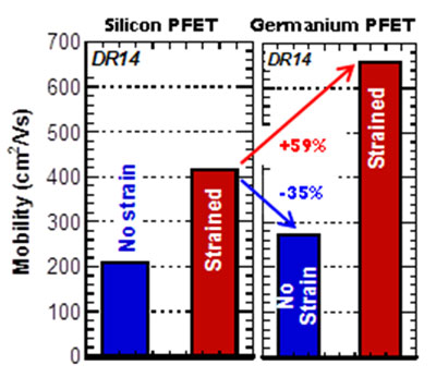
For logic device technology, the industry previously used SiGe source/drain stressors to enhance the Si channel mobility. However, this process is reaching its scalability limits due to lay-out dependent defects. At IEDM 2012, imec demonstrated excellent scalability toward the 1nm/10nm and 7nm nodes with Ge-channel FinFETs through a Si fin replacement process. Imec also delivered significant mobility boosts (of at least 50 percent) when growing a Ge channel on a SiGe 75 percent localized strain relaxed buffer, compared to strained Si channels.
|
 |
| Comparison of mobility in unstrained and strained Si and Ge p-FinFETs. Unstrained Ge shows degraded mobility w.r.t. strained Si. Strained Ge can improve pFET mobility by 59%.
|
|
Whereas recent work resulted in the reduction of the density of oxide-semiconductor interface traps of III-V and Ge MOS devices, imec presented new evidence of additional trapping of carriers, namely in the gate dielectrics of these non-Si devices. For the first time, imec showed the adverse impact of such oxide border traps on device performance. Imec’s research revealed that near-interface (fast) oxide traps can be probed using the AC-gm (AC transconductance) technique. Shallow (fast) oxide traps are believed to be responsible for non-Si MOSFET on-state frequency-dependent transconductance. This, in violation of the frequency invariance pre-requisite, can post a significant problem at circuit level. Imec also mapped out the slow border traps in the high-k dielectrics using the TSCIS (Trap Spectroscopy by Charge Injection and Sensing) technique. Imec demonstrated the charging of slower traps in the high-k dielectric, resulting in a drifting threshold voltage. As a result, a very low overdrive voltage is predicted (Ge/212mV, InGaAs/255mV, ~1/3 of the ITRS spec on Si) for the 10 year-lifetime of devices. Charge interaction with oxide border traps remains a challenge when moving toward non-Si devices.
|
|
“With each new technology generation, challenges are immense. And imec has always come up with solutions to extend Moore’s law,” stated Aaron Thean, director logic program at imec. “Moving on towards the 14nm node and beyond, we are confident that again, we will find solutions for the challenges that lie ahead. We are looking into high-mobility channel materials, such as Ge and III/V compounds, focusing on two main challenges namely how to implement non-Si materials into the device architecture and how to overcome some of the fundamental physics of the gate stack related to passivation.”
|
|
These results were obtained in cooperation with imec’s key partners in its core CMOS programs: Globalfoundries, INTEL, Micron, Panasonic, Samsung, TSMC, Elpida, SK Hynix, Fujitsu, Toshiba/Sandisk, and Sony.
|

