| Mar 11, 2013 | |
Nanotechnology on a megascale |
|
| (Nanowerk News) Eric Louis has been doing research into advanced multi-layer mirrors used for computer chips, among other things, for more than 20 years. This is nanotechnology in its truest sense, because each layer is only a few nanometres thick. However, this is done on a mega scale, because the mirrors can be up to one metre in size. The accuracy required for this is unprecedented: “In macroscopic terms it is as if you would cover the whole of the Netherlands with a layer of asphalt of 50 cm thickness while at no place in the country the deviation is allowed to be more than the thickness of an A4.” | |
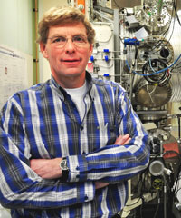 Eric Louis In order to explain his research, Louis first has to explain how computer chips are made. “This takes place in an optic process. Just as you can project a slide on a wall in larger dimensions, you can also make a reduced image of something.” The designer of a chip makes a pattern on a mask that you subsequently reduce using a lens and then project onto a light-sensitive layer on a chip. Since components for chips have to be increasingly smaller and you can make smaller images using shorter wavelengths of the light, the industry uses increasingly shorter wavelengths. Louis: “In the course of years, the industry has moved from visible light to ultraviolet light and now even deep ultraviolet. However, that is the last piece of the spectrum for which you are still able to make lenses. At an even shorter wavelength, all the light is absorbed.” Mirrors To overcome this problem, Louis and his fellow researchers focus light using concave and convex mirrors. However, this immediately leads to the next problem: these mirrors must be able to reflect sufficient light and there is no material that can do this. But there is a solution to this, too, for if you pile many reflecting surfaces onto one another, you can ensure that all these layers reflect a small part of the light, as a result of which the total reflection is large enough. The trick, according to Louis, lies in making these layers. “You must ensure that the distances between the reflecting surfaces properly fit in with the wavelength of the light. We use light with a wavelength of 13.5 nanometres, and therefore need to make layers 2-3 nanometres thick.” We need to work extremely accurately, especially because the dimensions of the mirrors, in terms of nanotechnology, can be huge, i.e. up to 1 metre in size. Louis: “It is as if you were to cover the whole of the Netherlands with a layer of asphalt of 50 cm thickness while at no place in the country the deviation is allowed to be more than the thickness of an A4.” |
|
| “What fascinates me in this is that it is extremely hard to imagine that you can make layers of 10 to 20 atoms thickness that have and retain the properties of the separate materials. And that you can make them in such a way that they are extremely flat, do not sustain any damage due to radiation, do not oxidise, do not bend due to material stress and a few other things that we have studied over the past 20 years. What gives me a great deal of satisfaction is that our research, although fundamental, is actually applied directly. Not only in the chips industry, incidentally. Our mirrors are also used for example for equipment that performs material analyses using X-rays, in aerospace research and for optic components with synchrotrons and X-ray free-electron lasers.” | |
| Doctoral thesis | |
| Louis recently obtained a PhD at the University of Twente. In doing so, he did not follow the most obvious academic path. Most people who do a PhD do so much earlier in their career and merely have a few scientific publications in their name. By now, Louis has more than 20 years of research experience. He has published 56 scientific articles and was himself involved in the supervision of approximately 20 doctoral researchers. “Now the time was right, I thought. I’m quite ambitious in achieving the best result: the right mirror for the right application. However, I may be a little less ambitious in the personal sphere. By this I mean that I found my work more important than seeking isolation to write my own book. Last year I was asked to write an extensive review article about our work. I accepted this invitation with both hands. This article was a proper basis to start my doctoral thesis with and to supplement it with material not previously published. The PhD feels like the circle is now complete.” | |
| Top of the bill | |
| Louis is currently still working at the FOM Institute DIFFER in Nieuwegein. The entire group that he is part of will move to the UT (here you can find more information about this). Louis looks forward to his new work environment. “For this particular field I consider the UT’s MESA+ institute top of the bill. Therefore we are really looking forward to continuing our work there.” |
| Source: University of Twente |