| Jun 12, 2013 |
New quantum dot technique combines best of optical and electron microscopy
|
|
(Nanowerk News) It's not reruns of "The Jetsons", but researchers working at the National Institute of Standards and Technology (NIST) have developed a new microscopy technique that uses a process similar to how an old tube television produces a picture—cathodoluminescence—to image nanoscale features. Combining the best features of optical and scanning electron microscopy, the fast, versatile, and high-resolution technique allows scientists to view surface and subsurface features potentially as small as 10 nanometers in size.
|
|
The new microscopy technique, described in the journal AIP Advances ("High-resolution photocurrent microscopy using near-field cathodoluminescence of quantum dots"), uses a beam of electrons to excite a specially engineered array of quantum dots, causing them to emit low-energy visible light very close to the surface of the sample, exploiting so-called "near-field" effects of light. By correlating the local effects of this emitted light with the position of the electron beam, spatial images of these effects can be reconstructed with nanometer-scale resolution.
|
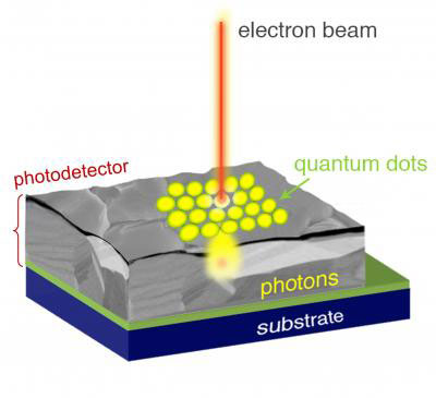 |
| Much like in an old tube television where a beam of electrons moves over a phosphor screen to create images, the new microscopy technique works by scanning a beam of electrons over a sample that has been coated with specially engineered quantum dots. The dots absorb the energy and emit it as visible light that interacts with the sample at close range. The scattered photons are collected using a similarly closely placed photodetector (not depicted), allowing an image to be constructed. (Image: Dill/NIST)
|
|
The technique neatly evades two problems in nanoscale microscopy, the diffraction limit that restricts conventional optical microscopes to resolutions no better than about half the wavelength of the light (so about 250 nm for green light), and the relatively high energies and sample preparation requirements of electron microscopy that are destructive to fragile specimens like tissue.
|
|
NIST researcher Nikolai Zhitenev, a co-developer of the technique, had the idea a few years ago to use a phosphor coating to produce light for near-field optical imaging, but at the time, no phosphor was available that was thin enough. Thick phosphors cause the light to diverge, severely limiting the image resolution. This changed when the NIST researchers teamed with researchers from a company that builds highly engineered and optimized quantum dots for lighting applications. The quantum dots potentially could do the same job as a phosphor, and be applied in a coating both homogenous and thick enough to absorb the entire electron beam while also sufficiently thin so that the light produced does not have to travel far to the sample.
|
|
The collaborative effort found that the quantum dots, which have a unique core-shell design, efficiently produced low-energy photons in the visible spectrum when energized with a beam of electrons. A potential thin-film light source in hand, the group developed a deposition process to bind them to specimens as a film with a controlled thickness of approximately 50 nm.
|
|
Much like in an old tube television where a beam of electrons moves over a phosphor screen to create images, the new technique works by scanning a beam of electrons over a sample that has been coated with the quantum dots. The dots absorb the electrons' energy and emit it as visible light that interacts with and penetrates the surface over which it has been coated. After interacting with the sample, the scattered photons are collected using a closely placed photodetector, allowing an image to be constructed. The first demonstration of the technique was used to image the natural nanostructure of the photodetector itself. Because both the light source and detector are so close to the sample, the diffraction limit doesn't apply, and much smaller objects can be imaged.
|
|
"Initially, our research was driven by our desire to study how inhomogeneities in the structure of polycrystalline photovoltaics could affect the conversion of sunlight to electricity and how these devices can be improved," says Heayoung Yoon, the lead author of the paper. "But we quickly realized that this technique could also be adapted to other research regimes, most notably imaging for biological and cellular samples, wet samples, samples with rough surfaces, as well as organic photovoltaics. We are anxious to make this technique available to the wider research community and see the results."
|