Showing Spotlights 561 - 568 of 631 in category All (newest first):
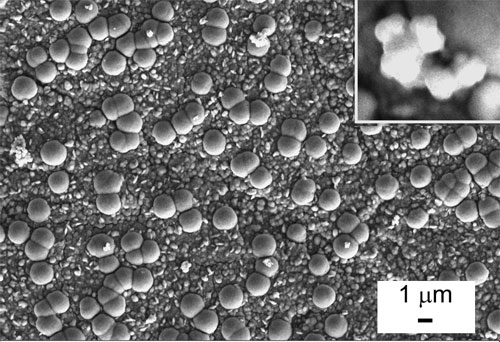 While many dynamic systems are lubricated by fluids of various kinds, modern technologies, like aerospace, clean room equipment, medical devices and machines, require the application of dry coatings which exhibit reduced friction and wear. Lubrication of dynamic surfaces by fluids adds complexity, weight and cost to the system, which imposes various constraints and limits the performance of these systems. Self-lubricating coatings, i.e. coatings which exhibit reduced wear and friction without resorting to tribological fluids, have been known for many years and are in use for a variety of applications. Numerous studies have shown that different nanoparticles, impregnated into metal, polymer, ceramic and other coatings, can provide these materials with enhanced tribological performance. Prominent among these additives are the fullerene-like (IF) nanoparticles of tungsten disulfide (WS2) and molybdenum disulfide (MoS2). New research shows that it is possible to obtain self-lubrication of hard (i.e. dry) coatings such as cobalt by impregnating fullerene-like nanoparticles of WS2 in such coatings. The coating serves as a reservoir of nanoparticles which are slowly released from the surface and provide easy shear and reduced oxidation of the coating or native metal surface, which is a common phenomenon in tribology (friction and wear) of metallic surfaces.
Feb 21st, 2007
 Nanoparticles are of great scientific interest as they are effectively a bridge between bulk materials and atomic or molecular structures. Nanoparticles that consist of crystals of tens to thousands of atoms have been synthesized and used as "artificial atoms". In order to develop nanoparticle-based devices, though, it is essential to be able to control the placement of nanoparticles relative to one another. Two- and three-dimensional crystals of nanoparticles can be generated in a relatively straightforward manner, but it has been impossible to direct the assembly of the particles with any degree of specificity. The problem is that nanoparticle assembly so far has been constrained by the isotropic interactions between the particles. Isotropic materials have identical values of a property in all crystallographic directions, i.e. they are almost spherical in appearance. Though it is increasingly evident that nanoparticles would become a much more powerful research and engineering tool if it were possible to to enable directional assembly, breaking the interaction symmetry in isotropic materials is a major challenge. Doing so would enlarge the scope of potential applications, because anisotropic assemblies, where the interatomic bond strengths is directionally dependent, have distinctive properties that cannot be found or produced in isotropic assemblies. Researchers at MIT now have reported a simple method to fabricate divalent metal nanoparticles. This work is a first step towards enabling the controllable, directional assembly of nanoparticles into more complex and well-specified structures.
Feb 7th, 2007
 The combination of sp3, sp2, and sp hybridized atoms can give rise to a large number of carbon allotropic forms and phases, starting from carbon crystals based on all sp3 (diamond) and sp2 (graphite, fullerene) are well known and characterized. In addition there are innumerable transitional forms of carbon where sp2 and sp3 hybridization bonds coexist in the same solid such as in amorphous carbon, carbon black, soot, cokes, glassy carbon, etc. Solids based on sp hybridization, although subject of intense experimental efforts, seem to be the most elusive of the different carbon families. Such one-dimensional (1D) structures - "real" carbon nanowires - are linear chains of carbon atoms linked by alternating single and triple bonds (polyynes) or only double bonds (polycumulene). They are considered the building blocks for the elusive "carbyne": an ideal crystal constituted by carbon atoms with sp hybridization only. In solid and stable form this would represent a new carbon allotrope whose existence was a matter of great debate in the 1980s. With the immense interest in carbon nanomaterials, sp carbon nanostructures have become objects of renewed interest in recent years since they are considered precursors in the formation of fullerenes and carbon nanotubes; moreover they are interesting in astrophysics since they are considered constituents of interstellar dust. 1D carbon nanowires are expected to show interesting optical, electrical and mechanical properties. Some techniques already permit the synthesis of linear carbon chains in solution. However, their extremely high reactivity against oxygen - they can literally explode - and a strong tendency to interchain crosslinking makes synthesis of pure carbyne solids a major challenge. Researchers in Italy have now presented a simple method to obtain a solid system where polyynes in a silver nanoparticle assembly display long-term stability at ambient conditions.
Feb 5th, 2007
Micro-and/or nano-electromechanical systems (MEMS/NEMS) are the basis of future nanotechnology, because they combine miniature sensors and actuators with electronics. The selection of appropriate materials for MEMS/NEMS fabrication is based on the careful consideration of a material's properties with regard to its intended application. For example, many MEMS devices, such as pressure, chemical and bio sensors, rely on actuation of a membrane structure and require a high fracture toughness material for the enhanced durability and shock resistance. On the other hand, for fabrication of controlled nanostructures, the material should be machinable up to atomic level. Currently, the materials used for MEMS/NEMS fabrication are based on silicon or oxides, which are brittle and have size effects such as lattice defects, anisotropy, grains and grain boundaries. These effects are the limiting factors in the reduction of pattern size, especially when a dimension of the pattern approaches a few tenths of a nanometer. Researchers in Japan now have introduced zirconium-based glass thin films for the fabrication of 3D micro- and nanostructures. These materials exhibit excellent micro/nano-formability under very low stresses, and are expected to become one of the most useful materials for fabricating NEMS/MEMS devices.
Jan 26th, 2007
The precise positioning of nanoparticles on surfaces is key to most nano- technology applications especially molecular electronics. However, for automated patterning of particles, existing methods are either slow (e.g., dip-pen lithography) or require prefabricated patterns (e.g., by electrostatic positioning or by successive self-assembly, transfer, and integration). Moreover, the sorting of differently sized particles, organelles, and cells in microfluidic networks is important for many biological and medical applications. Purely size-based sorting would offer the greatest control, but an automated method so far does not exist. Researchers in Switzerland now have discovered that acoustic streaming leads to sorting of particles dependent on their size. Nanoparticles aggregate at the antinodes and micrometer-sized particles aggregate on the nodes of oscillation patterns on micro- machined cantilevers. These surprising results open new possibilities for the sorting of nanoparticles.
Jan 24th, 2007
Nanowires are expected to play an important role in the emerging fields of nanoelectronics and nanooptics. In particular, the permanently growing complexity of integrated circuit designs requires a further reduction of the size of IC components that nanowires could facilitate. Nanowires are also a possible candidate for future functional nanostructures in plasmonic devices, i.e. for information (light) propagation and manipulation below the optical diffraction limit. For these purposes, cobalt disilicide (CoSi2) is a very promising contact material due to its extremely useful properties such as low resistance, its metallic behavior, its low lattice mismatch to Si of only -1.2%. the plasmon wavelength of 1.2 micrometer, and its compatibility with modern silicon technology. Many efforts have been made to fabricate silicide nanowires employing the bottom-up approach without elaborate microlithography. Researchers in Germany now have demonstrated a promising technique that allows the defect-induced formation and placing of cobalt disilicide nanowires by focused ion beam synthesis in silicon directly where it is needed.
Jan 22nd, 2007
Novel and robust networks, tailored from nanostructures as building blocks, are the foundations for constructing nano- and microdevices. However, assembling nanostructures into ordered micronetworks remains a significant challenge in nanotechnology. The most suitable building blocks for assembling such networks are nanoparticle clusters, nanotubes and nanowires. Unfortunately, little is known regarding the different ways networks can be created and their physicochemical properties as a function of their architecture. It is expected that, when 1D nanostructures are connected covalently, the resulting assemblies possess mechanical, electronic, and porosity properties that are strikingly different from those of the isolated 1D blocks. In extensive theoretical studies, researchers now have shown that the properties of 2D and 3D networks built from 1D units are dictated by the specific architecture of these arrays. Specifically, they demonstrate that one could join nanotubes and make supernetworks that exhibit different properties when compared to the individual building blocks (i.e. the nanotubes). Besides the unique and unusual mechanical and electronic properties, the porosity of these systems makes them good candidates for exploring novel catalysts, sensors, filters, or molecular storage properties. The crystalline 2D and 3D networks are also expected to present unusual optical properties, in particular when the pore periodicity approaches the wavelength of different light sources, such as optical photonic crystals.
Jan 4th, 2007
With its historic development tracing back to the Bronze Age, welding serves modern industry in broad areas such as construction, manufacturing, and engineering. Spot welding,a type of resistance welding used to weld various sheet metals, was originally developed in the early 1900s. The process uses two shaped copper alloy electrodes to concentrate welding current and force between the materials to be welded. The result is a small "spot" that is quickly heated to the melting point, forming a nugget of welded metal after the current is removed. Perhaps the most common application of spot welding is in the automobile industry, where it is used almost universally to weld the sheet metal forming a car. Spot welders can also be completely automated, and many of the industrial robots found on assembly lines are spot welders. With the continuing development of bottom-up nanotechnology fabrication processes, with self-assembly at its core, spot welding may likewise play an important role in interconnecting carbon nanotubes (CNTs), nanowires, nanobelts, nanohelixes, and other nanomaterials and structures for the assembly of nanoelectronics and nanoelectromechanical systems (NEMS).
Jan 2nd, 2007
 Subscribe to our Nanotechnology Spotlight feed