| Posted: Jan 26, 2007 |
Metallic glass promises to become a useful material for nanotechnology fabrication |
| (Nanowerk Spotlight) Micro (MEMS) and/or nano-electromechanical systems (NEMS) are the basis of future nanotechnology, because they combine miniature sensors and actuators with electronics. The selection of appropriate materials for MEMS/NEMS fabrication is based on the careful consideration of a material’s properties with regard to its intended application. |
| For example, many MEMS devices, such as pressure, chemical and bio sensors, rely on actuation of a membrane structure and require a high fracture toughness material for the enhanced durability and shock resistance. On the other hand, for fabrication of controlled nanostructures, the material should be machinable up to atomic level. |
| Currently, the materials used for MEMS/NEMS fabrication are based on silicon or oxides, which are brittle and have size effects such as lattice defects, anisotropy, grains and grain boundaries. These effects are the limiting factors in the reduction of pattern size, especially when a dimension of the pattern approaches a few tenths of a nanometer. Researchers in Japan now have introduced zirconium-based glass thin films for the fabrication of 3D micro- and nanostructures. These materials exhibit excellent micro/nano-formability under very low stresses, and are expected to become one of the most useful materials for fabricating NEMS/MEMS devices. |
| "Our results demonstrate the importance of metallic glasses as a new material for nanoscale fabrication" Dr. Parmanand Sharma explains to Nanowerk. "We were able to demonstrate the nanoscale fabrication (∼12nm) ability of metallic glass thin films using focused ion beam as well as using nanoimprint lithography techniques. The glassy metals posses many attractive properties such as higher fracture toughness, high corrosion resistance, atomically flat surface, and isotropic behavior, which are useful for the fabrication of nanoscale small structures. Besides this, the metallic glass thin films also posses other functional properties such as magnetism." |
| Sharma, a researcher at the Institute for Materials Research at Tohoku University in Japan, and his colleagues' motivation for this research was to find a suitable material which can allow easy and cost effective fabrication at the nanoscale. Tohoku University is home to a dedicated Advanced Research Center of Metallic Glasses. |
| "Our group (group leader Prof. Akihisa Inoue) has been working on bulk metallic glasses since they were developed" says Sharma. "In our present study we developed thin films of glassy metals on different substrates (such as silicon, silicon dioxide, polymers), and studied their nanoscale fabrication ability. Our results show that these very fine and stable metallic glassy nanoscale structures are integrable with silicon IC technology and can be fabricated on a large area using simple and cost effective techniques such as imprint lithography." |
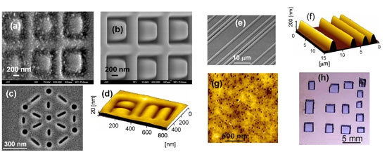 |
| Fabrication of nano/micro-patterns by direct writing using FIB on (a) Nanocrystalline FePtB, effect of granular structure on the fabrication ability of the material can be noticed, (b) amorphous FePtBZr, (c) & (d) glassy Zr-Al-Cu-Ni thin films; (e), (f) & (g) patterns made on glassy Zr-Al-Cu-Ni thin films by imprint lithography technique, where super-cooled liquid region of glassy metals was utilized. It is to be noted that pure metals or crystalline alloys do not exhibit supercooled liquid region therefore they can not be patterned directly using imprint lithography; and (h) Glassy thin film membrane on silicon made by anisotropic etching of silicon, and shows that glassy films has very good chemical stability in KOH (potassium hydroxide), and these membrane can be further utilized for fabrication of various types of sensors. (Image: Dr. Sharma/Tohoku University) |
| The metallic glass thin films could turn out to be basic building blocks for the fabrication of NEMS. Although researchers have demonstrated the fabrication of below 100 nm structures with current materials, the fabrication methods are not cost effective. For example, ∼20 nm sized features have been achieved on quartz to make a mold for imprint lithography. The insulating nature of quartz imposes a lot of restrictions during fabrication and inspection of the mold, and a thin layer of chromium is needed to suppress the charging during the e-beam exposure. Loss of critical dimensions during etching of the chromium layer makes fabrication very difficult. Moreover, the brittle nature of oxides and nitrides also make handling and fabrication of MEMS/NEMS devices difficult. |
| The glassy material introduced by the Japanese researchers is free from these defects and, in addition, possesses a temperature range where it can be molded into any desired shape even in the nanoscale range. |
| Sharma points out that glassy metals have relatively high electrical resistivity as compared to their crystalline counterparts. "We need to search for an alloy composition which possesses a lower electrical resistivity, and a lower value of glass transition temperature, with a large region of super-cooled liquid. The magnetic metallic glasses are soft magnetic; if we can find a glassy composition which exhibits a hard magnetic properties, this will broaden the area of applications." |
| Sharma and his colleagues are optimistic that within five years functional devices will be developed with metallic glass thin films by exploiting their promising chemical, mechanical and surface properties along with excellent nanoscale fabrication ability. |
| "As metallic glass has no crystal structure, it is possible to vary the average atomic distance between different kinds of atoms by proper dilution with other atoms, and therefore it is possible to tailor its functional properties" says Sharma. "For example, our recent studies on magnetic metallic glass thin films showed that the Curie temperature can be tailored from the temperature of liquid helium to above 450°K by appropriate dilution. Moreover the spin direction from inplane to out of plane can be changed, and the transition temperature at which this occurs can be tailored from the liquid helium temperature to room temperature." |
| Such a wide range for tailoring the functional properties is not possible with conventional materials. For Sharma and his colleagues the challenge now is to search for new alloy compositions and to find ways to tailor their functional properties according to the desired applications. |
| These findings have been reported in Nanotechnology: "Nano-fabrication with metallic glass—an exotic material for nano-electromechanical systems". |
| Previous work leading up to these recent findings were published in " Nanoscale Patterning of Zr-Al-Cu-Ni Metallic Glass Thin Films Deposited by Magnetron Sputtering" and " Temperature and thickness driven spin-reorientation transition in amorphous Co-Fe-Ta-B thin films". |
 By
Michael
Berger
– Michael is author of four books by the Royal Society of Chemistry:
Nano-Society: Pushing the Boundaries of Technology (2009),
Nanotechnology: The Future is Tiny (2016),
Nanoengineering: The Skills and Tools Making Technology Invisible (2019), and
Waste not! How Nanotechnologies Can Increase Efficiencies Throughout Society (2025)
Copyright ©
Nanowerk LLC
By
Michael
Berger
– Michael is author of four books by the Royal Society of Chemistry:
Nano-Society: Pushing the Boundaries of Technology (2009),
Nanotechnology: The Future is Tiny (2016),
Nanoengineering: The Skills and Tools Making Technology Invisible (2019), and
Waste not! How Nanotechnologies Can Increase Efficiencies Throughout Society (2025)
Copyright ©
Nanowerk LLC
|

Become a Spotlight guest author! Join our large and growing group of guest contributors. Have you just published a scientific paper or have other exciting developments to share with the nanotechnology community? Here is how to publish on nanowerk.com.
