| Posted: Jan 04, 2007 |
Designing new materials with nanostructures as building blocks |
| (Nanowerk Spotlight) Novel and robust networks, tailored from nanostructures as building blocks, are the foundations for constructing nano- and microdevices. However, assembling nanostructures into ordered micronetworks remains a significant challenge in nanotechnology. The most suitable building blocks for assembling such networks are nanoparticle clusters, nanotubes and nanowires. Unfortunately, little is known regarding the different ways networks can be created and their physicochemical properties as a function of their architecture. It is expected that, when 1D nanostructures are connected covalently, the resulting assemblies possess mechanical, electronic, and porosity properties that are strikingly different from those of the isolated 1D blocks. In extensive theoretical studies, researchers now have shown that the properties of 2D and 3D networks built from 1D units are dictated by the specific architecture of these arrays. Specifically, they demonstrate that one could join nanotubes and make supernetworks that exhibit different properties when compared to the individual building blocks (i.e. the nanotubes). Besides the unique and unusual mechanical and electronic properties, the porosity of these systems makes them good candidates for exploring novel catalysts, sensors, filters, or molecular storage properties. The crystalline 2D and 3D networks are also expected to present unusual optical properties, in particular when the pore periodicity approaches the wavelength of different light sources, such as optical photonic crystals. |
| The power of theoretical calculations at predicting novel materials with enhanced electronic and mechanical properties, using single atoms as building blocks, has been demonstrated repeatedly. A further step in this direction is to analyze the mechanical properties of 3D arrays built up from carbon nanotubes and study the influence of different framework architectures. |
| "With our recent work we provide new information related to the mechanical and electronic properties of 2D and 3D networks using carbon nanotubes (CNTs) as building blocks" Professor Mauricio Terrones explains to Nanowerk. "The blocks are joined covalently using heptagonal, octagonal and pentagonal carbon rings. The networks we propose could adopt a hexagonal lattice (supergraphite), a tetragonal network (super diamond), a cubic 3D network (super cubic) and a squared lattice (super square)." |
| Terrones, who is a member of the Advanced Materials Department at IPICyT in Mexico, and his colleagues from IPICyT and the Oak Ridge National Laboratory in Tennessee, observed that the damping properties of these nanotube networks are excellent and therefore their work motivates further experimental research. |
| "From an electronic point of view we realized that we could make networks with semiconducting and metallic tubes and therefore, we could guide electronic current through specific paths of the networks" he says. "The idea of having 3D electronic nanocomponents is quite exciting and we believe that in the future scientists will be able to make these materials." |
| Jose Manuel Romo-Herrera, a PhD student in Terrones' group, and first author of the paper published on these findings ("Covalent 2D and 3D Networks from 1D Nanostructures: Designing New Materials"), hopes that their simulations will motivate experimental work in the field in order to explore different types of geometries by selfassembly in order to "tune up" different type of properties to the arrays. |
| "Testing the properties of different 2D and 3D arrays was possible thanks to a hierarchy algorithm which is a simple set of rules to follow in order to design whichever ordered network, build up from a choice of constructor blocks" he explains. "To design the networks, we begin by selecting a 1D nanostructure as a building block, and by using point group operations we generated a multi-terminal node. Subsequently, we introduced the concept of hierarchy to use these nodes as the new building blocks, which by translation operations will result in complex architectures. These conceptual steps (illustrated with CNTs in the figure below) represent the hierarchy algorithm able to generate crystallographically different types of 2D and 3D supercrystal models from 1D blocks." |
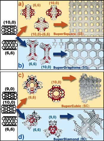 |
Illustrations of the hierarchy concept for four different architectures of ordered networks based on CNTs (1D nanostructures). (a and b) super-square and super-graphene correspond to 2D networks, whereas (c and d) super-cubic and super-diamond represent 3D network examples. The four families are constructed from either armchair or zigzag CNTs in order to study the chirality effects. The red rings point out the nonhexagonal carbon rings in each node.(Reprinted with permission from the American Chemical Society) |
| The researchers also demonstrated that the active surface area of these arrays could be as high as 3600 m2/gr and with densities much lower that than of water. |
| Romo-Herrera adds that this idea or algorithm should help the scientific community to design new types of networks and with different types of 1D nanostructures (inorganic nanowires, CNTs, doped CNTs, nanorods) in order to explore the different properties the arrays could present by "virtually playing Lego". |
| "Presenting our tools and results we are proposing a way of how to build new materials" says Terrones. "We propose to construct new materials with properties that are attractive in various areas such as catalysis (larger surface area porous materials with low densities), electronics (new 3D molecular devices), composites (fabrication of shock absorbers), and optoelectronics (porous materials with controllable holes that could interact with different wavelengths)." |
| This work could lead to a significant body of research, exploring the vast number of combinations of architectures and nanostructures and determining their respective mechanical and electronic properties. |
| "It provides the foundation for building new materials by connecting covalently 1D units" adds Terrones. "I personally believe that in less than 5 years materials like these will be produced with some control." |
 By
Michael
Berger
– Michael is author of four books by the Royal Society of Chemistry:
Nano-Society: Pushing the Boundaries of Technology (2009),
Nanotechnology: The Future is Tiny (2016),
Nanoengineering: The Skills and Tools Making Technology Invisible (2019), and
Waste not! How Nanotechnologies Can Increase Efficiencies Throughout Society (2025)
Copyright ©
Nanowerk LLC
By
Michael
Berger
– Michael is author of four books by the Royal Society of Chemistry:
Nano-Society: Pushing the Boundaries of Technology (2009),
Nanotechnology: The Future is Tiny (2016),
Nanoengineering: The Skills and Tools Making Technology Invisible (2019), and
Waste not! How Nanotechnologies Can Increase Efficiencies Throughout Society (2025)
Copyright ©
Nanowerk LLC
|

Become a Spotlight guest author! Join our large and growing group of guest contributors. Have you just published a scientific paper or have other exciting developments to share with the nanotechnology community? Here is how to publish on nanowerk.com.
