| Mar 29, 2024 |
An ultrafast method for producing large, uniform graphene glass in open air |
| (Nanowerk Spotlight) Graphene, a single layer of carbon atoms arranged in a two-dimensional honeycomb lattice, has captivated researchers since its discovery due to its extraordinary properties. However, the path to realizing graphene's full potential has been hindered by the challenges associated with producing large, high-quality graphene films in a cost-effective and scalable manner. |
| Over the past decade, chemical vapor deposition (CVD) has emerged as the primary method for growing high-quality, continuous graphene films. Despite notable advancements, such as the synthesis of foot-long single-crystal graphene films and the production of 4-inch single-crystal graphene wafers in just 10 minutes, the CVD method still faces limitations in terms of efficiency and uniformity due to the complex synthesis conditions required. Growing large-area, uniform graphene films remains a significant challenge, particularly when it comes to meeting the demands of industrial-scale production. |
| In a recent breakthrough, a team of researchers from the CAS Key Laboratory for Biomedical Effects of Nanomaterials and Nanosafety at the National Center for Nanoscience and Technology in Beijing, China, has developed a novel method for growing graphene that overcomes many of the limitations associated with traditional CVD techniques. Their scanning electromagnetic induction (SEMI) quenching method enables the ultrafast synthesis of large-sized, uniform graphene glass in open air, without the need for a vacuum chamber or catalyst. |
| The research has been published in Advanced Functional Materials ("Highly Efficient Growth of Large-Sized Uniform Graphene Glass in Air by Scanning Electromagnetic Induction Quenching Method"). |
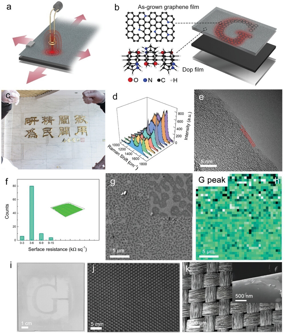 |
| Introduction of the SEMI method and thus-produced large sized uniform graphene glass.a)The illustration of the home-built experimental system; b) Schematic diagram of the graphene formation mechanism by the SEMI method; c) A photograph of a 400 mm × 400 mm graphene glass; d) The representative Raman spectra collected at different area across the graphene film; e) High-resolution TEM (HR-TEM) image of the graphene film transferred onto a Cu grid; f) Surface resistance value distribution on a 60 mm × 50 mm area (collected from 100 points); g,h) Confocal SEM-Raman results; g) SEM image, and the inset is the HR-SEM image; h) Raman mapping of the G peak intensity; i) A photograph of a graphene pattern; j) A photograph of a graphene glass fiber texture; k) SEM image of the graphene glass fiber texture, and the inset is the SEM image of the surface of one fiber coated with continous films. (Reprinted with permission from Wiley-VCH Verlag) |
| The SEMI method works by using an electromagnetic induction instrument to rapidly heat a graphite plate, which is in close contact with a glass substrate coated with a thin layer of poly-dopamine (PDA). As the induction coil moves over the substrate, the glass is instantaneously heated, and a continuous graphene film forms on the surface along the path of the coil. This approach allows for the growth of graphene films without the size limitations imposed by a vacuum chamber, making it much more scalable than CVD. |
| Using the SEMI method, the researchers produced a 400 mm × 400 mm graphene glass in just 2 minutes, a significant improvement over CVD techniques. The resulting graphene glass exhibited excellent uniformity, film adhesion, and full coverage, with a surface resistance below 500 Ω sq-1, far lower than that of graphene produced by other methods. Additionally, the graphene glass demonstrated outstanding thermal stability, maintaining stable performance at temperatures up to 1000 °C, surpassing the stability of other transparent conductive materials like indium tin oxide (ITO) and platinum films. |
| The SEMI method offers several key advantages over CVD, including the ability to grow graphene at high temperatures in open air, a scanning approach that ensures uniform heating and cooling, and compatibility with roll-to-roll processing for flexible substrates. By eliminating the need for a vacuum chamber and catalyst, the SEMI method significantly reduces production time and costs while enabling the growth of graphene on substrates of virtually any size. |
| The potential applications of graphene glass are vast, spanning industries such as electronics, energy storage, aerospace, and medicine. In electronics, graphene glass could revolutionize the production of touch screens, flexible displays, and solar cells, offering superior transparency, conductivity, and durability compared to current materials. In the energy sector, graphene glass could enable the development of more efficient and lightweight batteries and supercapacitors. For aerospace and automotive applications, graphene glass could lead to the creation of stronger, lighter, and more thermally stable components. In medicine, graphene glass could be used to develop advanced biosensors, drug delivery systems, and even artificial organs. |
| As research into the SEMI method continues, further optimizations and scaling up of the process are expected to lead to even greater advancements in the production of graphene films. The successful demonstration of this technique on various glass substrates, including quartz, glass-ceramic, and glass fiber textures, highlights its versatility and potential for integration with existing manufacturing processes. |
| However, challenges remain in fully realizing the potential of the SEMI method. Further research is needed to optimize the process parameters, such as the composition of the PDA layer, the temperature, and the speed of the induction coil, to achieve the best possible graphene quality and uniformity. Additionally, while the SEMI method is highly scalable, work is still needed to develop the infrastructure and supply chains necessary for large-scale production. |
| Despite these challenges, the development of the SEMI quenching method represents a significant leap forward in the production of large-area, high-quality graphene films for industrial applications. By enabling the ultrafast growth of uniform graphene glass in open air, this innovative approach overcomes the limitations of traditional CVD methods and paves the way for the cost-effective, large-scale production of graphene-based devices. |
| In the coming years, as researchers continue to refine and optimize this groundbreaking technique, we can expect to see a new era of graphene-based technologies that leverage the extraordinary properties of this material to create transformative applications across a wide range of industries. The SEMI method brings us one step closer to realizing the full potential of graphene. |
 By
Michael
Berger
– Michael is author of four books by the Royal Society of Chemistry:
Nano-Society: Pushing the Boundaries of Technology (2009),
Nanotechnology: The Future is Tiny (2016),
Nanoengineering: The Skills and Tools Making Technology Invisible (2019), and
Waste not! How Nanotechnologies Can Increase Efficiencies Throughout Society (2025)
Copyright ©
Nanowerk LLC
By
Michael
Berger
– Michael is author of four books by the Royal Society of Chemistry:
Nano-Society: Pushing the Boundaries of Technology (2009),
Nanotechnology: The Future is Tiny (2016),
Nanoengineering: The Skills and Tools Making Technology Invisible (2019), and
Waste not! How Nanotechnologies Can Increase Efficiencies Throughout Society (2025)
Copyright ©
Nanowerk LLC
|

Become a Spotlight guest author! Join our large and growing group of guest contributors. Have you just published a scientific paper or have other exciting developments to share with the nanotechnology community? Here is how to publish on nanowerk.com. |
