| Apr 24, 2024 |
Mechanical strain control of quantum transport in graphene enables new class of nanoelectronic devices |
| (Nanowerk Spotlight) Controlling the flow of electrons through materials at the nanoscale is essential for the development of advanced electronics and quantum technologies. Scientists have long sought ways to precisely tune how electric current moves through two-dimensional materials like graphene, which consists of a single layer of carbon atoms. |
| The crystal structure of these atomically thin materials makes them extremely sensitive to mechanical strain – tiny stretches or compressions of the atomic lattice. In principle, this strain sensitivity could be harnessed to control their electronic properties, but achieving this in practice has proven challenging. |
| Now, a research team from Concordia University in Canada has developed a new experimental platform that allows them to apply precise mechanical strain to graphene devices while simultaneously measuring their electrical transport properties at low temperatures. This technical advance has enabled them to demonstrate unprecedented mechanical control over key quantum properties like graphene's work function, ballistic conductance, and quantum interference effects. |
| Their results, reported in Advanced Materials ("Mechanical Control of Quantum Transport in Graphene"), provide the first quantitative experimental validation of long-standing theoretical predictions and point the way toward a new class of strain-tunable nanoelectronic devices. |
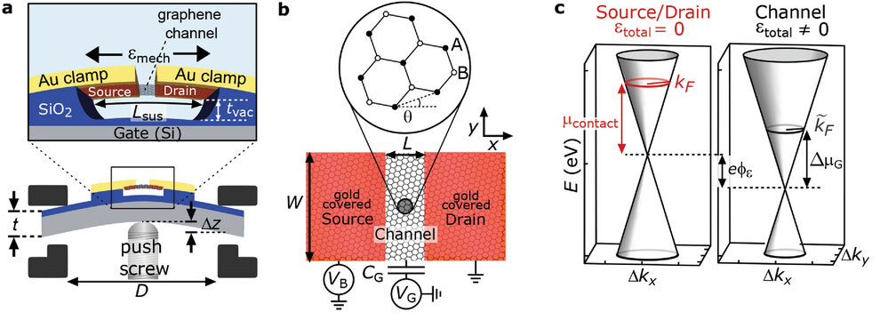 |
| Platform for strain-engineering of quantum transport in 2DMs: applied theory, custom instrumentation, and device design. a) Sample holder geometry showing the bending of a Si substrate hosting a suspended graphene transistor. b) Top-view diagram of the graphene transistor showing the source, channel, and drain regions. The inset shows the orientation 𝜃 of the crystal lattice with respect to the strain direction. c) Band structure in one valley of graphene’s first Brillouin zone (FBZ) in the source/drain (unstrained) and channel (strained). The vertical shift of the bands due to strain is εφε. (Image: Adapted from DOI:10.1002/adma.202313629, CC BY) |
| The intimate coupling between mechanical strain and electronic properties in two-dimensional materials has attracted intense research interest for both fundamental physics and potential technological applications. Scientists have proposed that strain could be used to continuously tune device characteristics, turn electrical currents on and off, or even alter exotic quantum phases of matter. However, progress has been hindered by the lack of methods to impose well-controlled strain fields while probing delicate quantum transport phenomena. |
| In this work, the researchers developed custom instrumentation and a device architecture to meet this challenge. They fabricated graphene devices with suspended channels anchored by gold electrodes, which were shaped into slender bridges and attached to a thin, bendable silicon substrate. By pushing on the back of this assembly with a finely threaded screw, they could stretch the graphene in a precise and tunable way, achieving strains as high as 2.6%. |
| Mounting their straining assembly in a cryogenic measurement system allowed the researchers to study the impact of strain on electron flow at temperatures near absolute zero, where quantum effects dominate. |
| A key finding was the ability to shift the energy of electron waves in the graphene channel relative to the unstrained contacts by applying strain, effectively tuning graphene's work function by up to 25 millielectronvolts. This mechanical modulation of the work function could prove useful for optimizing electrical contact to graphene in nanoscale devices. |
| Even more striking was the observation that strain could dramatically suppress graphene's ballistic conductance – the unimpeded flow of electrons through the channel in the absence of scattering. The researchers observed conductance reductions up to 30% under about 1% strain and found they could reversibly tune the effect by adjusting the strain in situ. Through careful comparison to theoretical modeling, they showed this conductance change originates from a specific strain-induced effect – the development of pseudo-magnetic vector potentials, which deflect the trajectories of the electrons. |
| The concept of generating vector potentials equivalent to magnetic fields through mechanical strain was first proposed theoretically for graphene in 2010. The theory predicted phenomena like conductance suppression, but experimental confirmation has remained elusive until now. The researchers' transport data quantitatively match these predictions, providing the first direct evidence of strain-generated vector potentials and demonstrating a new means to create and control them in devices. |
| As a further confirmation of this effect, the team observed signatures of the vector potentials in the interference patterns of the electron waves traveling through the strained graphene. Analogous to the famous Aharonov-Bohm effect, the strain-induced vector potential creates a phase shift in the wave interference, which the researchers detected as a systematic change in the pattern of quantum conductance oscillations. Their data again agreed with modeling based on the theory of strain-induced gauge fields in graphene. |
| The results demonstrate that by employing strain as a knob to control electron wave interference, phase-coherent transport can be modulated in graphene devices. Integrating this strain modulation with the ability to also tune the Fermi level using electrostatic gates, as the researchers have done, opens up the possibility of advanced quantum devices with dual electro-mechanical control. |
| The researchers suggest their strain-tuning platform could enable the exploration of unique device functionalities in various nanomaterials. For example, uniaxial strain could be used to induce a transition from a normal insulator to a topological quantum spin Hall insulator in certain two-dimensional crystals. Applying strain to superconducting materials like magic-angle twisted bilayer graphene could potentially be used to tune their critical temperature or manipulate novel electron pairing states. |
| More broadly, the ability to control quantum transport phenomena through mechanical deformation could impact the development of low power nanoelectronics and quantum computing hardware. Possibilities include mechanically gated transistors, strain-tunable qubits, and quantum transducers that convert between mechanical and electronic signals. With the potential to locally modify properties and break crystal symmetries, strain engineering expands the design space for quantum devices. |
| While this work represents a major step forward, challenges remain in developing strain-engineered quantum technologies. One limitation is that the strain fields are still not completely uniform at the nanoscale. Integrating strain control with the complex multilayer structures of practical devices will require further innovations in nanofabrication and strain characterization. |
| Nonetheless, by demonstrating quantitative agreement between theory and experiment, this work establishes a firm basis for future strain-engineered quantum devices. The results highlight the potential of mechanical strain as a versatile tool for controlling quantum materials and provide an important step toward harnessing the rich interplay of mechanics and electronics in nanoscale systems. |
 By
Michael
Berger
– Michael is author of four books by the Royal Society of Chemistry:
Nano-Society: Pushing the Boundaries of Technology (2009),
Nanotechnology: The Future is Tiny (2016),
Nanoengineering: The Skills and Tools Making Technology Invisible (2019), and
Waste not! How Nanotechnologies Can Increase Efficiencies Throughout Society (2025)
Copyright ©
Nanowerk LLC
By
Michael
Berger
– Michael is author of four books by the Royal Society of Chemistry:
Nano-Society: Pushing the Boundaries of Technology (2009),
Nanotechnology: The Future is Tiny (2016),
Nanoengineering: The Skills and Tools Making Technology Invisible (2019), and
Waste not! How Nanotechnologies Can Increase Efficiencies Throughout Society (2025)
Copyright ©
Nanowerk LLC
|

Become a Spotlight guest author! Join our large and growing group of guest contributors. Have you just published a scientific paper or have other exciting developments to share with the nanotechnology community? Here is how to publish on nanowerk.com. |
