Nanoscale: Definition, Size Range, and Why It Matters in Nanotechnology
What is the Nanoscale?
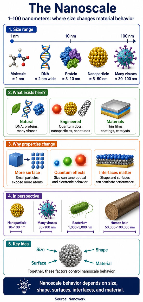
In one sentence: The nanoscale is the size range from roughly 1 to 100 nanometers, where matter is small enough that surfaces, interfaces, and quantum effects can reshape its physical and chemical properties.
The nanoscale is the length range, conventionally taken as approximately 1 to 100 nm, in which a material's properties often depend explicitly on its size, shape, and internal structure. The boundary is empirical rather than fundamental: different properties cross over from bulk-like to size-dependent behavior at different lengths.
A nanometer is one billionth of a meter, ten Ångströms, or about the width of ten hydrogen atoms placed in a row. The nanoscale begins near the size of small molecules and atomic clusters and extends to objects still far too small to resolve with an ordinary optical microscope. For comparison, DNA is about 2 nm wide, many proteins are a few to tens of nanometers across, many common viruses are roughly 30 to 100 nm in diameter, and a human hair is roughly 50,000 to 100,000 nm in diameter.
Key takeaways:
- The nanoscale is conventionally defined as approximately 1 to 100 nanometers.
- Its limits are practical conventions, not sharp natural borders.
- Properties change because surface atoms become a large fraction of the total and because nanoscale dimensions can match quantum-mechanical length scales.
- Size-dependent optical, electronic, magnetic, mechanical, and catalytic behavior often appears in this range.
- The nanoscale is central to nanoscience, modern semiconductor manufacturing, structural biology, catalysis, medicine, and advanced materials.
Size Range in Context
The internationally accepted nanotechnology vocabulary describes the nanoscale as the length range approximately from 1 nm to 100 nm. The word "approximately" matters. A 120 nm virus, a 150 nm polymer particle, or a sub-nanometer atomic cluster can still show behavior that is best discussed with nanoscale concepts. Conversely, not every object between 1 and 100 nm automatically has useful or unusual properties. The important point is not only size, but whether the relevant physical, chemical, or biological length scale has become comparable to the object's dimensions.
| Scale | Approximate size | Examples |
|---|---|---|
| Atomic and molecular scale | Below about 1 nm | Atoms, small molecules, chemical bonds |
| Nanoscale | About 1 to 100 nm | DNA width, many proteins, quantum dots, nanoparticles, many viruses |
| Submicron scale | About 100 nm to 1 µm | Large viruses, fine particles, small cellular structures |
| Microscale | Usually about 1 to 100 µm, depending on context | Bacteria, blood cells, many cells, micromechanical structures |
The submicron range is the bridge between nano and micro. This is why the transition from nanoscale to microscale should not be treated as a hard line at exactly 100 nm. One micrometer equals 1,000 nm, so micrometer-scale objects are already far larger than the conventional nanoscale range, but the physical crossover can be gradual.
Why Properties Change at the Nanoscale
Two effects explain most nanoscale behavior. The first is geometric: surfaces and interfaces become dominant. The second is quantum mechanical: electrons, excitons, phonons, or magnetic domains may be confined by dimensions comparable to their natural length scales.
The geometric effect is captured by the surface-to-volume ratio. For a sphere of diameter d, surface area scales as d2 and volume as d3, so surface-to-volume ratio scales as 1/d. As particles shrink, a much larger fraction of atoms sit at surfaces or interfaces. These atoms have fewer bonded neighbors, different energies, and different chemical environments than atoms in the interior. That change can alter melting temperature, reactivity, catalytic activity, solubility, and mechanical strength.
Gold illustrates the point. Bulk gold melts at about 1064 °C and is chemically rather inert. Gold nanoparticles only a few nanometers across can have much lower melting temperatures, sometimes falling to a few hundred degrees Celsius depending on size and environment. Gold nanoparticles can also become highly active for reactions such as low-temperature carbon monoxide oxidation when divided into particles only a few nanometers across and supported on suitable oxides.
The quantum mechanical effect is captured by quantum size effects. When a crystal becomes smaller than the natural length scale of the electronic wavefunctions it contains, electrons can no longer always be treated as occupying continuous bands. Discrete energy levels appear, and their spacing depends on size. In semiconductor nanocrystals, this produces a size-tunable bandgap: the same material can emit different colors at different diameters. In metallic nanoparticles, collective electron oscillations produce surface plasmon resonances. In magnetic nanoparticles below a material-dependent critical size, magnetic domains can collapse into single-domain or superparamagnetic behavior.
Examples Across Material Systems
Different materials show different nanoscale signatures. Colloidal gold nanoparticles roughly 5 to 50 nm in diameter can appear ruby red because their plasmon absorption depends on size, shape, and local environment. Engineered plasmonic nanostructures use the same physics in colorimetric biosensors, photothermal therapies, and surface-enhanced Raman spectroscopy.
In semiconductors, quantum dots of CdSe, InP, lead halide perovskites, and related materials often fall in the 2 to 20 nm range. Their emission color can be tuned by diameter, which is why quantum dots are used in display backlights, fluorescent bioimaging probes, and emerging optoelectronic devices. Carbon materials show a different kind of nanoscale diversity: fullerenes are about 1 nm across, single-walled carbon nanotubes are often 1 to 2 nm in diameter, graphene is one atom thick, and graphene nanoribbons can acquire width-dependent electronic properties.
Catalysts often rely on metal or ceramic nanoparticles in the 1 to 10 nm range because small particles expose many atoms to reactants. In structural metals, refining grains from micrometers to tens of nanometers can increase strength through Hall–Petch strengthening, although very small grains may introduce additional deformation mechanisms. Biology also operates heavily at the nanoscale: DNA is about 2 nm wide, many proteins and antibodies are a few to tens of nanometers across, ribosomes are roughly 20 to 30 nm, and influenza viruses are about 80 to 120 nm.
Significance in Nanotechnology
The nanoscale is the natural meeting point of chemistry, condensed-matter physics, materials science, and biology. It is also the working domain of nanotechnology: the deliberate measurement, design, synthesis, patterning, and integration of structures whose useful behavior depends on nanometer-scale dimensions.
Two engineering strategies organize much of the field. Top-down nanotechnology starts with larger pieces of material and uses lithography, etching, deposition, and milling to make nanoscale features. This route underpins the semiconductor industry. Advanced logic chips are manufactured with transistor features and gate structures whose critical dimensions are measured in nanometers, even though commercial node names no longer correspond directly to literal physical feature sizes. Bottom-up nanotechnology builds structures from atoms, ions, molecules, or particles using colloidal synthesis, self-assembly, atomic layer deposition, and chemical vapor deposition.
Working at this scale requires tools matched to it. Ordinary optical microscopes are limited by diffraction to features above roughly 200 nm, so nanoscale imaging and measurement rely heavily on electron microscopy, scanning probe microscopy, X-ray scattering, spectroscopy, and related methods. The scanning tunneling microscope, invented in 1981, made routine atomic-resolution imaging of conducting surfaces possible and later enabled controlled manipulation of individual atoms. Together with transmission electron microscopy and atomic force microscopy, it made nanoscale structures directly measurable rather than merely theoretical.
Future progress in nanotechnology is likely to depend less on simply making things smaller and more on controlling structure, composition, interfaces, and assembly with high precision. Atomically precise clusters, quantum defects, quantum dots, nanostructured catalysts, lipid nanoparticles, and nanoscale semiconductor devices all show the same lesson: at nanometer dimensions, small structural differences can produce large functional differences.
FAQ: The Nanoscale
How big is the nanoscale exactly?
The internationally accepted nanotechnology vocabulary places the nanoscale at approximately 1 to 100 nanometers. The limits are useful conventions, not hard natural borders. Some size-dependent effects appear below 1 nm or above 100 nm, depending on the material and property being measured.
What is the difference between the nanoscale and the microscale?
The nanoscale is about 1 to 100 nm. The microscale is usually associated with dimensions from about 1 to 100 micrometers, although usage varies by field. The submicron range between 100 nm and 1 micrometer bridges the two. Nanoscale objects are distinctive because surface atoms and quantum length scales strongly influence their properties.
Why do materials behave differently at the nanoscale?
Two effects dominate. First, the surface-to-volume ratio rises sharply as objects get smaller, so surface atoms and interfaces can control melting, reactivity, solubility, and catalysis. Second, nanoscale dimensions can become comparable to quantum-mechanical length scales such as exciton Bohr radii, electron wavelengths, or mean free paths, making optical, electronic, and magnetic behavior depend on size.
Are nanoscale objects man-made or also found in nature?
Both. Engineered nanomaterials are produced industrially, but nature is full of nanoscale objects and structures, including DNA, proteins, ribosomes, many viruses, soot, sea-spray aerosols, and the nanostructures that give butterfly wings and opals their structural colors. The defining feature is size and architecture, not origin.
Further Reading
Chemical Society Reviews, Size matters: why nanomaterials are different
Nature Materials, The surface science of nanocrystals
