Understanding Scanning Tunneling Microscopy for Precise Surface Analysis
Definition: Scanning Tunneling Microscopy (STM) is a powerful nanoscale imaging technique capable of providing atomic-level resolution of surface structures. By utilizing the quantum mechanical phenomenon of electron tunneling, STM allows for the direct observation of individual atoms and molecules on a material's surface, making it a cornerstone tool in the fields of nanotechnology, surface science, and materials engineering.
Principle of Operation
The fundamental principle behind STM is the quantum tunneling effect, where electrons can move between two conductors separated by an insulating barrier, in this case, the vacuum gap between the tip and the sample. By maintaining the tip's position close to the surface and scanning it across the sample, the STM maps the surface topography at the atomic level based on variations in the tunneling current.
How Scanning Tunneling Microscopy Works
An extremely sharp conducting tip, often made of tungsten or platinum-iridium, is brought within a few angstroms to the sample surface. A bias voltage applied between the tip and the sample causes electrons to tunnel across the gap, creating a measurable current. The tip's position is meticulously adjusted using piezoelectric controls to maintain a constant tunneling current, allowing the device to image surfaces with atomic precision.
Key Features of Scanning Tunneling Microscopy
STM is celebrated for its remarkable features:
- Atomic Resolution: STM's most notable feature is its ability to image surfaces at the atomic scale, providing unparalleled insights into the structural and electronic properties of materials.
- Surface Modification: Beyond imaging, STM can also manipulate individual atoms and molecules on a surface, enabling the fabrication of nanostructures and devices directly on the atomic scale.
- Versatility: STM can be applied to a wide variety of conductive and semiconductive materials, including metals, semiconductors, and certain types of insulators when coated with a conductive layer.
- Real-Time Imaging: STM allows for the real-time observation of dynamic processes on the surface, such as diffusion, adsorption, and molecular rearrangements.
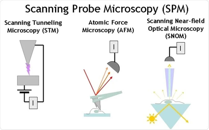
Relation to Scanning Probe Microscopy and Other Techniques
Scanning Tunneling Microscopy is a subset of Scanning Probe Microscopy (SPM), a group of techniques that image and manipulate surfaces at the nanometer to atomic scales. SPM techniques share the common approach of scanning a probe over a specimen's surface to gather information.
- Atomic Force Microscopy (AFM): Atomic Force Microscopy, another prominent SPM technique, uses a cantilever with a sharp tip to physically touch the surface and measure the force between the tip and the sample. Unlike STM, AFM can image non-conductive materials, making it more versatile for a broader range of samples.
- Scanning Near-field Optical Microscopy (SNOM): SNOM combines optical microscopy with nanoscale scanning to overcome the diffraction limit of conventional optical microscopy. By illuminating the sample through a tiny aperture at the end of a sharp probe, SNOM provides optical images with nanometer resolution, applicable to a wide range of materials, including insulators.
While STM provides unparalleled atomic-resolution images of conductive and semiconductive surfaces, AFM and SNOM extend the capabilities of SPM to non-conductive materials and offer complementary information such as mechanical, electrical, and optical properties at the nanoscale. Together, these techniques provide a comprehensive toolkit for surface analysis across diverse scientific fields.
The synergistic use of STM, AFM, and SNOM enables researchers to obtain a more complete understanding of material properties, facilitating advancements in nanotechnology, materials science, and beyond.
Applications of Scanning Tunneling Microscopy
The unique capabilities of STM have led to its widespread use across multiple scientific domains:
- Material Science: STM is indispensable for studying surface structures, defects, and electronic properties of materials, aiding in the development of new materials with tailored properties.
- Nanotechnology: In nanotechnology, STM is used to construct and analyze nanostructures and devices, playing a crucial role in the advancement of nanoscale electronics and quantum computing.
- Surface Chemistry: STM provides detailed insights into chemical reactions at surfaces, including the observation of reaction intermediates and pathways at the atomic level.
- Biology: Although less common, STM can image biological molecules like DNA and proteins under specific conditions, contributing to molecular biology and bioengineering.
Advancements and Future Directions
Ongoing advancements in STM technology, including the development of low-temperature and high-vacuum systems, have expanded its application range and improved its resolution and sensitivity. The integration of STM with other spectroscopic methods enhances its analytical capabilities, promising new insights into the atomic-scale phenomena governing material and biological systems.
Environmental and Industrial Impacts
STM's ability to precisely analyze surface phenomena has implications for environmental science, catalysis, and semiconductor industry, where understanding surface interactions at the molecular level can lead to more efficient catalytic processes, improved environmental sensors, and the development of next-generation electronic devices.
Further Reading
Nanomaterials, Scanning Tunneling Microscopy of Biological Structures: An Elusive Goal for Many Years
Electrochemical Energy Reviews, Application of Scanning Tunneling Microscopy in Electrocatalysis and Electrochemistry
