Understanding Scanning Near-field Optical Microscopy in Nanotechnology
Introduction to SNOM: The Scanning Near-field Optical Microscope (SNOM) stands as a pivotal analytical tool in nanotechnology, enabling the visualization of nanostructures with resolution beyond the diffraction limit of light. This technique bridges the gap between optical microscopy and nanoscale imaging, offering insights into material properties at the nanometer scale.
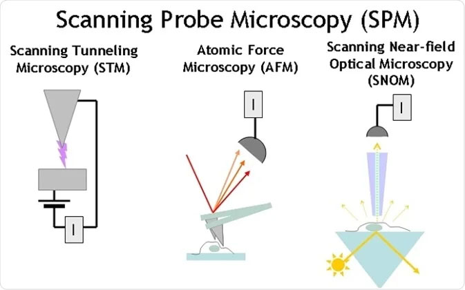
Principle and Mechanism
SNOM operates on the principle of near-field scanning optical microscopy, where a small aperture or sharp tip scans across the sample surface at a nanometric distance. Unlike traditional optical microscopy, SNOM bypasses the diffraction limit by exploiting the near-field, the non-propagating electromagnetic field existing within a few nanometers of the surface. This method enables the visualization of surface features with unprecedented detail and resolution.
Comparison with AFM, STM, and SPM
While SNOM shares similarities with Atomic Force Microscopy (AFM), Scanning Tunneling Microscopy (STM), and Scanning Probe Microscopy (SPM) in terms of scanning mechanisms, it uniquely provides optical and spectroscopic information about the sample. AFM and STM are confined to topographical and electronic properties, respectively. In contrast, SNOM combines the high spatial resolution of SPM techniques with the ability to discern optical properties, making it invaluable for studying a wide array of materials including biological specimens, polymers, and nanostructured materials.
Key Advantages of SNOM
- High Spatial Resolution: SNOM exceeds the optical diffraction limit, offering spatial resolution in the order of tens of nanometers.
- Optical Property Analysis: Unlike AFM and STM, SNOM can provide detailed optical and spectroscopic data, such as fluorescence or Raman scattering, from the sample surface.
- Versatile Sample Compatibility: SNOM can analyze a wide range of materials, from insulators to biological specimens, without the need for conductive coatings or extensive sample preparation.
- Non-destructive Evaluation: The technique is minimally invasive, preserving the integrity of sensitive samples during analysis.
Applications and Impact
SNOM has revolutionized how scientists study materials at the nanoscale, with applications in photovoltaics, semiconductor research, biological imaging, and beyond. Its ability to map optical properties with high resolution has opened new avenues in nanophotonics, plasmonics, and materials science.
The ongoing development of SNOM technology, including improved tip designs and enhanced detection methods, continues to expand its capabilities and applications, solidifying its role as a cornerstone technique in nanotechnology.
