Understanding Scanning Probe Microscopy for Nanoscale Analysis
Definition: Scanning Probe Microscopy (SPM) is a branch of microscopy that forms images of surfaces using a physical probe that scans the specimen. SPM is instrumental in the analysis and characterization of surfaces at the nanometer scale, offering insights into the physical, chemical, and topographical properties of materials.
Principles Behind Scanning Probe Microscopy
At its core, SPM operates on the principle of measuring interactions between a sharp probe and the surface of a material. As the probe scans across the surface, it detects variations in physical properties such as force, capacitance, or tunneling current, which are translated into detailed topographical images.
How Scanning Probe Microscopy Works
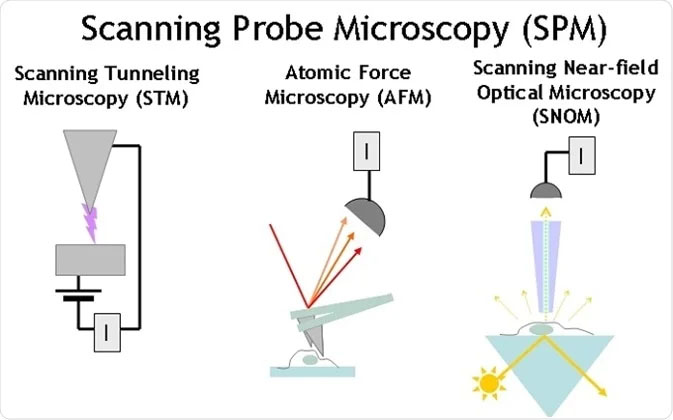
SPM encompasses a variety of techniques, each based on different interactions between a probe and the surface of a material. The most common forms include Atomic Force Microscopy (AFM), which measures force interactions, Scanning Tunneling Microscopy (STM), which relies on tunneling current between the probe and the surface, and Scanning Near-field Optical Microscopy (SNOM), which offers optical imaging at resolutions beyond the diffraction limit of light.
These techniques measure variations in physical properties such as force, capacitance, tunneling current, or light intensity as the probe scans across the surface. These variations are meticulously recorded and mapped, producing high-resolution images of the surface at the atomic or molecular level. SNOM, in particular, combines the high-resolution capabilities of SPM with the rich spectroscopic information provided by optical microscopy, enabling detailed studies of optical properties at the nanoscale, which is invaluable for investigating photonic devices, biological specimens, and nanomaterials.
Advantages of Scanning Probe Microscopy
- Atomic Resolution: SPM techniques, particularly STM and AFM, can achieve atomic-scale resolution, enabling the visualization of individual atoms and molecules on surfaces.
- Versatility: SPM can be used with a wide variety of materials, including conductors, semiconductors, and insulators, without the need for special treatments or environments.
- Quantitative Measurements: Beyond imaging, SPM can provide quantitative measurements of physical properties such as mechanical stiffness, electrical conductivity, and magnetic forces.
- Operational in Various Environments: SPM can be performed in various environments, including vacuum, air, and liquid, allowing for the study of biological specimens and chemical reactions in situ.
Applications of Scanning Probe Microscopy
SPM's ability to provide detailed surface characterization at the nanoscale makes it invaluable in numerous fields:
- Nanotechnology: SPM is crucial in the development and characterization of nanomaterials and nanodevices, facilitating advancements in electronics, photonics, and material science.
- Material Science: It helps in understanding material properties, such as hardness, friction, and wear, at the nanoscale, influencing the development of new materials.
- Life Sciences: In biology and medicine, SPM is used to image cells and biomolecules, aiding in the understanding of biological processes and the development of pharmaceuticals.
- Energy Research: SPM techniques are used to study energy-related materials and devices, including photovoltaic materials and battery electrodes, contributing to the development of renewable energy technologies.
Technological Advancements in Scanning Probe Microscopy
Innovation in SPM continues to expand its capabilities, including the integration of SPM techniques with other microscopy and spectroscopy methods, the development of high-speed scanning probes for dynamic studies, and the use of advanced algorithms for data analysis, enhancing both the resolution and the range of applications.
Recent breakthroughs in probe design and imaging techniques have also allowed for the exploration of new phenomena at the nanoscale, pushing the boundaries of what can be visualized and measured with SPM.
Environmental and Industrial Monitoring
SPM's sensitivity to surface properties makes it a powerful tool for detecting and analyzing contaminants and wear in industrial and environmental contexts, contributing to the development of more durable materials and cleaner technologies.
Advancing Scientific Research
The continuous advancements in SPM techniques are opening new avenues for scientific discovery, enabling researchers to probe the nanoworld with unprecedented precision and depth.
Further Reading
Nature Reviews Methods Primers, Scanning Probe Microscopy
Nature Reviews Methods Primers, Scanning Probe Microscopy: From Sublime to Ubiquitous
