| Apr 07, 2024 |
Tunable quantum dot microcavities could unlock scalable quantum photonics |
| (Nanowerk Spotlight) In the efforts to develop quantum computers and secure communication networks, a tiny device called a single photon source is a crucial component. By emitting light as a stream of individual photons, these sources can generate the quantum bits, or qubits, that form the foundation of quantum information technologies. However, making single photon sources that are efficient, reliable and scalable has proven enormously challenging, limiting progress in the field. |
| A team of researchers from China reports a significant advance that could finally overcome this bottleneck. Writing in Light: Science & Applications ("Tunable quantum dots in monolithic Fabry-Perot microcavities for high-performance single-photon sources"), they describe a new type of single photon source based on a quantum dot embedded in a purpose-designed microcavity. By integrating several key innovations, their device achieves a combination of performance metrics that has long been sought but never before demonstrated. |
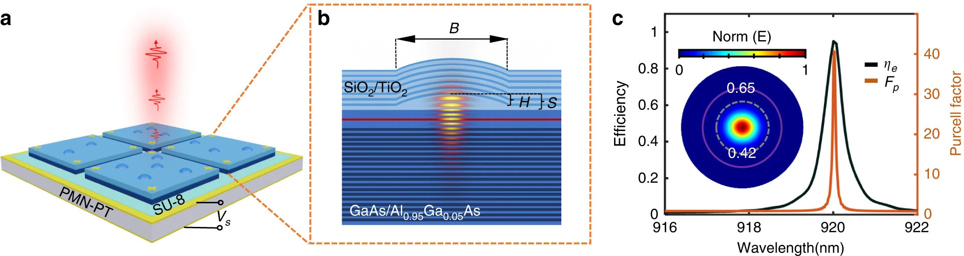 |
| a Sketch of tunable single photon source. Transferable Fabry-Perot microcavity integrated with PMN-PT (100) substrate by SU-8. b Cross-section of monolithic Fabry-Perot microcavity and electric field distribution of fundamental mode. The vertical confinement is from two mirrors: The top one is a dielectric SiO2/TiO2 distributed Bragg reflector (DBR), while the bottom one consists of GaAs/AlGaAs DBR. The lateral confinement is provided by the parabolic lensed-defect in the central spacer layer. Here, B is the base width of lensed defect, H is the height and S is the thickness of total SiO2 spacer. The InAs/GaAs QD is positioned at the field maximum within the GaAs microcavity. c. Three-dimensional simulation result of the microcavity. Extraction efficiency ηe of ~0.949 and Purcell factor Fp of ~40 are obtained in device with B = 4 µm, H = 350 nm, and S = 480 nm for 7-pairs top DBR. Inset is the far-field distribution showing near Gaussian profile. Dotted gray and solid purple circles represent NA = 0.42 and NA = 0.65, respectively. (Image: Light: Science & Applications, CC BY) |
| At the heart of the device is a quantum dot, a nanoscale island of semiconductor that can emit single photons when excited by a laser. Quantum dots are a leading platform for single photon sources, but they suffer from several problems. First, only a small fraction of the emitted photons can usually be collected, with the rest leaking out at random angles. Second, variations between individual dots lead to unpredictable emission wavelengths. Finally, interactions with the surrounding material can reduce the indistinguishability of the emitted photons, a key requirement for quantum applications. |
| To solve these issues, the researchers turned to a tried-and-true approach: embedding the quantum dot in an optical cavity. Like a microscopic hall of mirrors, a cavity can trap and amplify light, directing it into a useful output. If the cavity is precisely tuned to resonate with the quantum dot emission, a phenomenon called the Purcell effect occurs, boosting the rate of photon emission while also improving directionality and indistinguishability. |
| Quantum dot cavity designs have been explored previously, but they all have drawbacks. Open cavities are highly sensitive to vibration and take up a lot of space. Designs etched directly from semiconductor material, like micropillars, provide stability but are difficult to fabricate around selected quantum dots. The new microcavity aims to overcome these limitations by combining novel fabrication methods with an optimized optical design. |
| The device consists of two mirrors made from alternating layers of dielectric material, forming what are called distributed Bragg reflectors. Between the mirrors is a spacer layer with a unique lens-shaped defect that serves to focus light in the center of the cavity. Embedded right at the focal point of this defect is a single quantum dot that has been pre-selected for its high quality. |
| The use of dielectric mirrors is a key innovation. Unlike earlier approaches based on semiconductor mirrors, dielectric materials can conformally coat the lens-shaped defect, maintaining a uniform cavity mode. This allows the cavity dimensions to be reduced to the scale of a few micrometers while still achieving a high quality factor, a measure of how well it traps light. A smaller cavity leads to stronger interaction with the quantum dot and a higher Purcell factor. |
| Just as important is how the researchers position the quantum dot at the cavity hotspot. Rather than searching for chance alignments in millions of devices, they use a technique called in-situ electron beam lithography to locate individual dots and then build cavities around them. This deterministic approach allows a massive improvement in yield and scalability. |
| Perhaps the most significant innovation is the integration of the cavity with a piezoelectric actuator. The mirrors and quantum dot are first grown on a sacrificial substrate, then transferred to the actuator as a thin flexible membrane. Applying a voltage to the actuator creates strain in the quantum dot layer, allowing its emission wavelength to be tuned by nearly a nanometer to match the cavity resonance. |
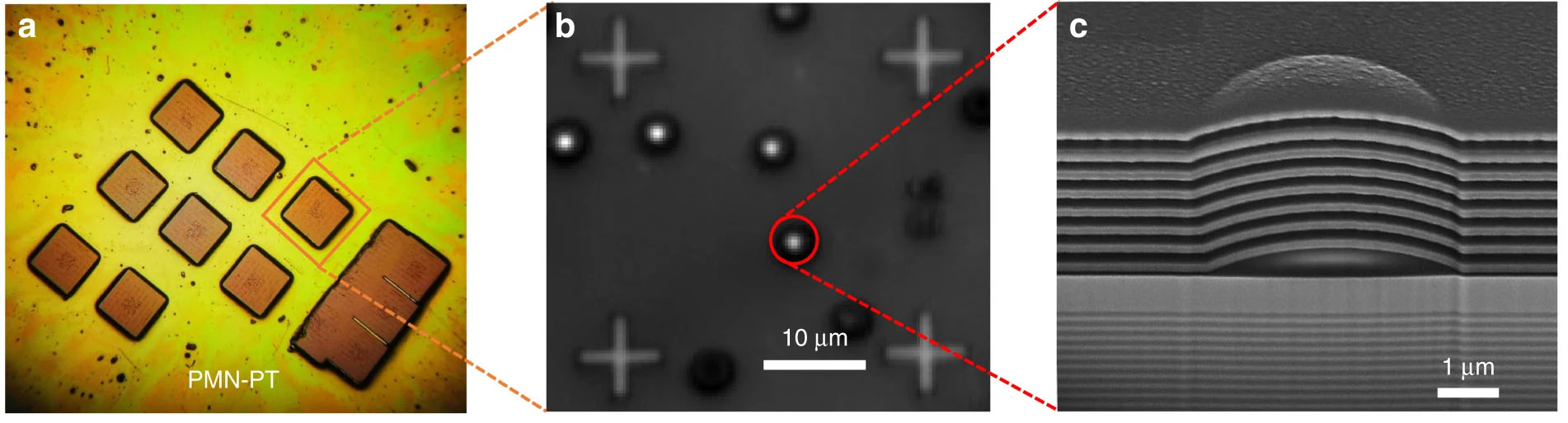 |
| a Integrated demo and cavity characterization. a Transferable films with cavities are glued to PMN-PT (100) substrate by SU-8 adhesive. Each square film is in size of ~280 μm× 280 μm. b Wide-field photoluminescence image of the fabricated Fabry-Perot microcavities with a single quantum dot in each center. The emissions from quantum dots (QDs) are excited by a high-power blue LED (445 nm), while the markers are illuminated by a white LED. The adjacent markers are separated by a distance of 30 μm. c Scanning microscope image of the cross-section of the cavity, which is milled by focus ion beam. The lens-shaped structure is maintained even after depositing an 8-pair dielectric DBR (~2 μm thick) on top. (Image: Light: Science & Applications, CC BY) |
| The wavelength tuning is crucial because even with precise positioning, tiny variations between quantum dots make it impossible to reliably match their emission to the cavity. Previous tuning methods involved changing the temperature or laser power, both of which can degrade the single photon emission. Strain tuning, on the other hand, preserves the pristine quantum properties of the dot. |
| The result of all these innovations is a single photon source that checks all the boxes for quantum technology applications. When the quantum dot is in perfect tune with the cavity, a nine-fold enhancement of photon emission occurs. This allows 58% of the generated single photons to be collected, a huge improvement over the few percent possible without a cavity. |
| At the same time, photon indistinguishability, a measure of how identical the photons are, reaches 92%. This is essential for quantum applications like cryptography and computing, which rely on photons being totally interchangeable. The photons are also strongly polarized, important for interfacing with other photonic components. |
| Just as impressive are the opportunities for scaling up the technology. Because the microcavity is built on a thin, flexible membrane, hundreds or thousands of them could potentially be combined on a single piezoelectric chip, with each cavity tuned to the same wavelength. This would enable the creation of large arrays of identical single photon sources, a critical step towards practical quantum computing. |
| Integration with electronic controls is also highly promising. By adding surface electrodes, it should be possible to precisely control the charge and spin state of the quantum dot. This could allow the entanglement of electron spins with emitted photons, a key capability for quantum networking. The quantum dots could also potentially serve as quantum memories to store and process information locally. |
| While there is still work to be done to optimize performance and scalability, the new strain-tunable quantum dot microcavity marks a major milestone for quantum light sources. By simultaneously achieving high efficiency, indistinguishability and scalability, it removes some of the biggest roadblocks on the path to practical quantum technologies. |
| More fundamentally, the device is a powerful demonstration of the ability to precisely engineer quantum states of light and matter at the nanoscale. As classical technologies rapidly approach the limits of miniaturization, the ability to harness quantum effects in microscopic devices will be crucial to continuing the pace of innovation in computing and communication. The strain-tunable microcavity shows how scientific ingenuity can build bridges across the gap between the quantum world and real-world applications. |
 By
Michael
Berger
– Michael is author of four books by the Royal Society of Chemistry:
Nano-Society: Pushing the Boundaries of Technology (2009),
Nanotechnology: The Future is Tiny (2016),
Nanoengineering: The Skills and Tools Making Technology Invisible (2019), and
Waste not! How Nanotechnologies Can Increase Efficiencies Throughout Society (2025)
Copyright ©
Nanowerk LLC
By
Michael
Berger
– Michael is author of four books by the Royal Society of Chemistry:
Nano-Society: Pushing the Boundaries of Technology (2009),
Nanotechnology: The Future is Tiny (2016),
Nanoengineering: The Skills and Tools Making Technology Invisible (2019), and
Waste not! How Nanotechnologies Can Increase Efficiencies Throughout Society (2025)
Copyright ©
Nanowerk LLC
|

Become a Spotlight guest author! Join our large and growing group of guest contributors. Have you just published a scientific paper or have other exciting developments to share with the nanotechnology community? Here is how to publish on nanowerk.com. |
