| Apr 22, 2024 |
Tiny crystals with a big impact on technology innovation |
| (Nanowerk Spotlight) In modern technology, the manipulation of various types of waves—including light, sound, electronic, and magnetic waves—is fundamental to advancing a wide range of applications. This manipulation is predominantly achieved through the design of periodic structures at the nanoscale, often referred to as nanostructured crystals. These crystals are engineered materials with precisely controlled periodic arrangements of their constituent elements, enabling them to interact with and control waves in ways that are not possible with conventional materials. |
Table of Contents
|
Exploring the Versatility of Nanostructured Crystals |
| The term crystal in this context does not necessarily refer to a traditional crystalline solid like salt or diamond, but rather to any material with a highly ordered, repeating structure at the nanoscale. These nanostructured crystals, through their precise periodicity and geometric arrangements, control how waves interact with materials, enabling selective enhancement, suppression, or redirection of specific wave frequencies. |
| Understanding the properties and applications of these various types of nanostructured crystals is crucial for anyone interested in the cutting-edge advancements in materials science, nanotechnology, and their impact on diverse fields such as optics, acoustics, electronics, and magnetics. This article aims to provide a comprehensive overview of the different types of nanostructured crystals, their unique properties, and their potential applications, bridging the gap between the fundamental science and real-world implications of these fascinating materials. |
| Periodic structures such as photonic crystals manipulate light waves to create highly efficient optical devices, while phononic crystals control sound waves for applications in noise reduction technologies. Similarly, electronic and magnetic waves are manipulated by structures like magnonic crystals, which are pivotal in the development of next-generation computing systems. |
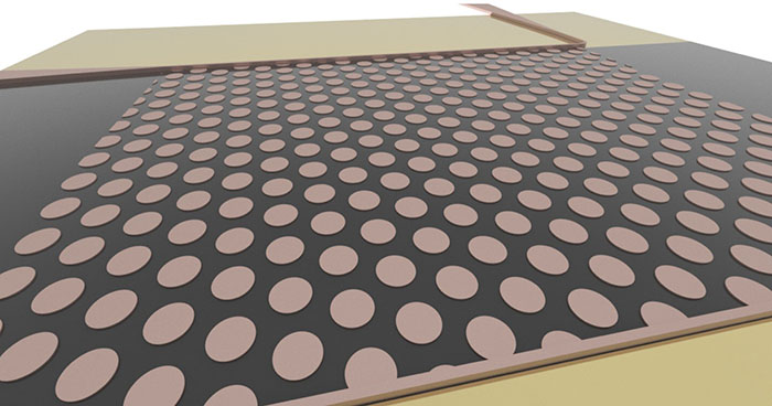 |
| An illustration of the two-dimensional magnonic crystal, viewed from an oblique angle. Copper disks are periodically arranged on a magnetic garnet film. (Image: Tohoku University) |
| The impact of these engineered materials is profound across various sectors. For example, photonic crystals are crucial in the development of high-efficiency solar cells that more effectively convert sunlight to electricity. In healthcare, phononic crystals are utilized in ultra-sensitive biosensors that detect diseases at much earlier stages. Moreover, in telecommunications, the use of these materials in optical fibers enhances signal clarity and speed, enabling high-speed optical communication systems. |
| By providing tailored pathways for wave propagation, these periodic structures not only enhance the performance of existing technologies but also drive the innovation of new applications that can transform industries. This ongoing research and development promise to yield further breakthroughs that enhance our ability to harness the power of wave-matter interactions at the microscopic level. |
Common Themes and Properties of Nanostructured Crystals |
| Before diving into the specifics of each type of nanostructured crystal, it is essential to understand the common themes and properties that unite these seemingly diverse materials. By exploring these shared characteristics, we can better appreciate the underlying principles that make these crystals such powerful tools for wave manipulation and their potential for transformative applications. |
Periodic Structures |
| The defining feature of nanostructured crystals is their periodic arrangement of constituent elements at the nanoscale. This periodicity can be in the form of alternating layers, repeating patterns, or precisely arranged nanostructures. The length scale of this periodicity is typically on the order of the wavelength of the waves these crystals are designed to manipulate, enabling strong wave-matter interactions. This precise control over the periodic structure is what sets nanostructured crystals apart from conventional materials and allows for the engineering of unique properties. |
Wave-matter interaction |
| Building upon the foundation of periodic structures, each type of nanostructured crystal is engineered to interact with specific types of waves, such as light, sound, electronic, or magnetic waves. The periodic structure of the crystal creates a unique environment for these waves, leading to phenomena such as bandgaps, where certain frequencies of waves are prohibited from propagating through the material. By tailoring the periodic structure, researchers can control and manipulate these wave-matter interactions with unprecedented precision, enabling applications ranging from perfect lenses and invisibility cloaks to ultra-efficient energy harvesting and quantum information processing. |
Tailored properties |
| The true power of nanostructured crystals lies in the ability to precisely tailor their properties by controlling their periodicity, geometry, and material composition. For example, the bandgap of a photonic crystal can be tuned by adjusting the size and spacing of its nanostructures, allowing researchers to create materials that selectively reflect or transmit specific colors of light. Similarly, the mechanical properties of a phononic crystal can be engineered by choosing materials with specific elastic constants and designing the appropriate periodic structure. This level of control over the properties of materials is unprecedented and opens up a vast design space for creating novel functionalities. |
Multidisciplinary applications |
| The versatility of nanostructured crystals lies in their ability to manipulate different types of waves, making them relevant to a wide range of scientific and technological disciplines. Photonic crystals, for instance, find applications in optical computing, energy harvesting, and telecommunications, while phononic crystals are employed in acoustic cloaking, vibration control, and ultrasonic imaging. This multidisciplinary nature of nanostructured crystals fosters collaboration among researchers from diverse fields, driving innovation and discovery. Recent breakthroughs, such as the development of topological photonic crystals that enable robust control of light propagation, highlight the exciting possibilities enabled by these materials. |
 |
| Left beam: Light propagation inside a photonic crystal is forbidden by a propagation gap. Hence common plane waves are reflected and hardly penetrate into the crystal. Right beam: By shaping the incident waves, one steers the waves deep into the crystal, thereby enabling the focusing of light at any desirable depth inside the otherwise forbidden gap. (Image: COPS, University of Twente) |
Fabrication techniques and challenges |
| The realization of nanostructured crystals relies on advanced fabrication techniques that enable the creation of intricate periodic structures with nanoscale precision. Lithographic methods, such as electron beam lithography and nanoimprint lithography, are commonly used to pattern these structures. Self-assembly techniques, where nanostructures spontaneously organize into periodic arrangements, provide another powerful approach for creating large-area nanostructured crystals. |
| However, fabricating these complex structures with high precision and uniformity remains a significant challenge, particularly for large-scale applications. Ongoing research focuses on developing scalable and cost-effective fabrication methods, such as high-throughput nanoimprint lithography and directed self-assembly, to overcome these limitations and bring the benefits of nanostructured crystals to real-world applications. |
| By understanding these common themes and properties, as well as the challenges and opportunities associated with nanostructured crystals, we can appreciate the fundamental principles that govern their behavior and their potential for transformative applications. As research in this field continues to advance, we can expect to see even more innovative solutions and breakthrough technologies enabled by these remarkable materials. With this foundation in place, we can now explore the specific types of nanostructured crystals and their unique properties in more detail. |
Harnessing Wave-Matter Interactions: The Power of Nanostructured Crystals |
Crystals for Optical Manipulation |
| Photonic Crystals |
|
Nonlinear Optical Crystals
|
Photorefractive Crystals
|
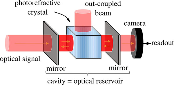 |
| A photorefractive crystal placed in a cavity. Light entering the cavity will interact with the photorefractive crystal such that part of the light will be coupled out of the cavity. Moreover, frequently occurring recurring patterns in the time-dependent input signal will interfere similarly in the crystal resulting in a form of self-learning. (Image: Reprinted from DOI:10.1038/s41598-021-81899-w, CC BY) |
Crystals for Hybrid Wave-Matter Interactions |
Plasmonic Crystals
|
Phoxonic Crystals
|
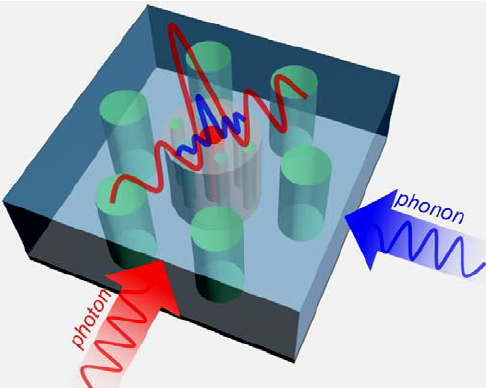 |
| Schematic of a portion of a 2D hierarchical phoxonic crystal with both large scale photonic lattice and a smaller scale phononic lattice inside a cavity resonator in the larger scale lattice. (Image: Adapted from Edwin L Thomas: "Final Report for AOARD Grant 1014069") |
Crystals for Mechanical and Acoustic Manipulation |
Piezoelectric Crystals
|
Phononic Crystals
|
Optomechanical Crystals
|
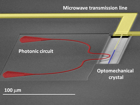 |
| Schematic of an optomechanical crystal coupled to a microwave transmission line. The optomechanical crystal (gray) contains a photonic circuit (red) that guides light waves. The microwave transmission line (yellow) allows coupling of microwave signals into the optomechanical crystal, where they can interact with the light waves and mechanical vibrations confined within the nanostructure. This enables the coherent transfer of information between the microwave and optical domains, which is crucial for applications in quantum information processing and sensing. (Image: Joerg Bochmann & Amit Vainsencher, UCSB) |
Crystals for Electronic and Magnetic Applications |
Ferroelectric Crystals
|
Magnonic Crystals
|
Crystals for Specialized and Emerging Applications |
Polaritonic Crystals
|
Superconducting Crystals
|
Topological Crystals
|
Future Possibilities and Multidisciplinary Applications |
| The field of nanostructured crystals is rapidly evolving, with new discoveries and advancements emerging at an unprecedented pace. As our understanding of these materials deepens and our ability to control their properties improves, the potential for groundbreaking applications across various disciplines becomes increasingly apparent. |
| One of the most exciting prospects lies in the development of multifunctional materials and devices that integrate multiple types of nanostructured crystals. By combining the unique properties of different crystals, researchers can create hybrid systems that exhibit novel functionalities and enhanced performance. For instance, the integration of photonic and phononic crystals could lead to the development of highly efficient optomechanical devices for sensing, signal processing, and quantum information applications. Similarly, the combination of plasmonic and ferroelectric crystals could enable the realization of ultracompact, tunable metamaterials with unprecedented control over light-matter interactions. |
| The integration of nanostructured crystals with other advanced materials, such as two-dimensional materials (e.g., graphene, transition metal dichalcogenides) and topological insulators, opens up new avenues for the design of innovative devices. For example, the integration of topological photonic crystals with two-dimensional materials could enable the development of robust, ultracompact optical circuits that are immune to defects and disorder. Moreover, the combination of superconducting crystals with topological materials could lead to the realization of fault-tolerant quantum computing architectures, paving the way for the development of large-scale, practical quantum computers. |
| In addition to the integration of different crystal types, the development of advanced fabrication techniques, such as 3D printing and self-assembly, will play a crucial role in the future of nanostructured crystals. These techniques enable the creation of complex, hierarchical structures with unprecedented control over their geometry and composition. By leveraging these advanced manufacturing capabilities, researchers can design and fabricate nanostructured crystals with tailored properties for specific applications, such as high-efficiency solar cells, ultra-sensitive biosensors, and compact quantum devices. |
| The multidisciplinary nature of nanostructured crystals also presents unique opportunities for collaboration and innovation across different fields. For instance, the integration of photonic crystals with microfluidic systems could revolutionize the field of lab-on-a-chip diagnostics, enabling the development of highly sensitive, miniaturized devices for point-of-care testing. Similarly, the combination of magnonic crystals with spintronics could lead to the development of ultra-low power, high-speed data processing devices that could transform the computing landscape. |
| Moreover, the application of machine learning and artificial intelligence techniques to the design and optimization of nanostructured crystals could accelerate the discovery of new materials with unprecedented properties. By leveraging the power of data-driven approaches, researchers can efficiently explore vast design spaces and identify novel crystal structures with tailored functionalities for specific applications. |
| The future of nanostructured crystals is highly promising, with the potential to transform a wide range of fields, from energy and healthcare to computing and telecommunications. The integration of different crystal types, along with the development of advanced fabrication techniques and the application of data-driven approaches, will undoubtedly lead to the emergence of new technologies and solutions to some of the most pressing challenges facing society today. As research in this field continues to advance, we can expect to see even more innovative applications and breakthroughs that will shape the future of technology and improve our daily lives. The possibilities are truly endless, and the exciting journey of discovering and harnessing the full potential of nanostructured crystals has only just begun. |
 By
Michael
Berger
– Michael is author of four books by the Royal Society of Chemistry:
Nano-Society: Pushing the Boundaries of Technology (2009),
Nanotechnology: The Future is Tiny (2016),
Nanoengineering: The Skills and Tools Making Technology Invisible (2019), and
Waste not! How Nanotechnologies Can Increase Efficiencies Throughout Society (2025)
Copyright ©
Nanowerk LLC
By
Michael
Berger
– Michael is author of four books by the Royal Society of Chemistry:
Nano-Society: Pushing the Boundaries of Technology (2009),
Nanotechnology: The Future is Tiny (2016),
Nanoengineering: The Skills and Tools Making Technology Invisible (2019), and
Waste not! How Nanotechnologies Can Increase Efficiencies Throughout Society (2025)
Copyright ©
Nanowerk LLC
|

Become a Spotlight guest author! Join our large and growing group of guest contributors. Have you just published a scientific paper or have other exciting developments to share with the nanotechnology community? Here is how to publish on nanowerk.com. |
