| Apr 19, 2024 |
New nondestructive technique for analyzing single-atom-thick materials |
| (Nanowerk Spotlight) Imagine a material 100,000 times thinner than a sheet of paper, yet stronger than steel, more conductive than copper, and with the potential to revolutionize everything from electronics to energy. This is the field of two-dimensional (2D) materials – a fascinating world where ordinary rules of physics and chemistry are rewritten at the atomic scale. |
| Since the groundbreaking isolation of graphene in 2004, the first 2D material consisting of a single layer of carbon atoms, researchers have been captivated by the extraordinary properties that emerge when bulk crystals are reduced to their thinnest possible form. Graphene's unmatched strength, electrical conductivity, and thermal properties quickly earned it the moniker of a "wonder material," prompting scientists to search for other atomically thin structures with similarly remarkable characteristics. |
| This exploration has uncovered a treasure trove of 2D materials, each with its own unique set of properties. From insulating hexagonal boron nitride and semiconducting transition metal dichalcogenides like molybdenum disulfide to exotic magnetic and superconducting 2D systems, these flatland materials offer an unprecedented opportunity to engineer novel functionalities at the atomic scale. |
| The applications are as diverse as they are transformative. In electronics, 2D materials could enable ultra-fast, low-power transistors and transparent, flexible displays. For energy storage, they could lead to high-capacity batteries and super-efficient solar cells. In the field of catalysis, 2D materials offer massive surface areas and tunable active sites for accelerating chemical reactions. And in the emerging field of quantum computing, certain 2D systems exhibit exotic states of matter that could form the basis of noise-resilient quantum bits. |
| Yet despite the immense promise, the path from lab to market has been challenging for 2D materials. One of the biggest obstacles has been the difficulty of precisely characterizing and controlling their atomic structure. |
| The arrangement of atoms, including grain boundaries and crystal orientations, plays a crucial role in determining the electrical, optical, chemical and mechanical characteristics of 2D materials. Historically, mapping out this microstructure has posed a formidable challenge. |
| The go-to tools for probing the atomic landscape of 2D crystals, such as transmission electron microscopy and scanning tunneling microscopy, can resolve individual atoms but only over minuscule areas. They also tend to be slow, expensive and require great technical skill to operate. |
| Other methods that exploit the selective reactivity of grain boundaries, like oxidation or nanoparticle deposition, can rapidly map the location of grains over larger regions. However, extracting the crystal orientations within those grains remains elusive. |
| Crucially, these established characterization techniques all share a critical flaw – they irreversibly damage or contaminate the delicate 2D samples. This renders the characterized material unusable for further studies or device fabrication, greatly limiting the utility of structural information obtained. For years, this restriction has hampered progress in 2D materials research, with the structure and properties of countless samples lost to the very tools used to analyze them. |
| Now, a team of researchers has devised an ingenious solution to this conundrum, described in a new study published in the journal Advanced Materials ("Nondestructive Single-Atom-Thick Crystallographic Scanner via Sticky-Note-Like van der Waals Assembling–Disassembling"). By harnessing the same weak van der Waals forces that bind layers of 2D materials together, they have demonstrated a nondestructive method to comprehensively map grain structure and crystal orientations over large areas, preserving the pristine quality of the original sample. |
| The key innovation lies in using a filter made from a single layer of high-quality, single-crystal graphene with a known orientation as a reference. An unknown sample, like a a polycrystalline graphene sheet, is placed on top of this filter to create a temporary stack. The interaction between the two layers alters their Raman scattering spectra in a way that depends sensitively on the relative twist angle of their crystal lattices. |
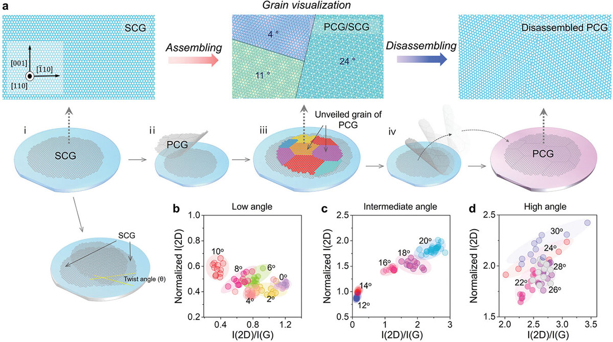 |
| 2D crystallographic scanning via vdW assembling and disassembling. a) Schematic of 2D crystallographic scanning process of PCG with four steps: i) SCG-filter preparation, ii) vdW assembling of the PCG with the SCG-filter, iii) crystallographic scanning, and iv) nondestructive disassembling of PCG from SCG. Following the crystallographic scan, the disassembled PCG can be transferred to another target substrate. b–d) The Raman spectral DB used for labeling the crystallographic orientation of scanned PCG’s grains. θ denotes the interlayer twist angle between two stacked layers of SCG. The plots depict the normalized I(2D) versus I(2D)/I(G) for: b) low twist angle (𝜃 < 10°), c) intermediate twist angle (10° < θ < 20°) and d) high twist angle (20° < θ < 30°). (Reprinted from DOI:10.1002/adma.202400091, CC BY) (click on image to enlarge) |
| By simply shining laser light on the stack and collecting the Raman signal, the researchers can map out the location and orientation of individual grains in the sample with sub-micron resolution. Boundaries between grains with different orientations show up as sharp color changes in the Raman images. The team validated their approach by correlating the twist angles inferred from Raman with direct measurements using electron diffraction. |
| Perhaps the most remarkable aspect is the reversibility afforded by the weak van der Waals bonding between layers. After imaging, the sample and reference filter can be peeled apart effortlessly without leaving behind residue or defects, much like a sticky note. Rigorous characterization of separated layers using atomic force microscopy, X-ray photoelectron spectroscopy and Raman mapping confirmed they remain unscathed by the process. |
| The implications are profound. Previously inaccessible 2D samples can now be scanned and then used for further experiments or applications, greatly increasing their research value. Transport measurements on a polycrystalline graphene film showed excellent mobility that varied predictably with the number of grain boundaries traversed, confirming no performance degradation. |
| In an ultimate demonstration of reusability, the authors performed repeated cycles of attaching an unknown sample to their graphene filter, mapping its grain structure, and then cleanly separating the layers. The same filter could be used again and again to analyze many different samples, with no impact on its own structural or optical integrity. |
| While the reported results focused on graphene, the weak interlayer coupling, and angle-dependent Raman signatures are common features of many 2D materials. Therefore, this new "sticky note" approach should be widely applicable to a variety of atomic membranes. Future research could extend the concept to artificial stacks assembled from different 2D building blocks. |
| By overcoming the destructive limitations of existing methods, this work opens the door to deep insights into the structure-property relationships of 2D materials. Researchers can now routinely access the crystallographic secrets locked within atomic sheets and leverage that knowledge to create designer materials with tailored grain sizes, shapes, and boundary configurations. Such precisely engineered 2D structures could deliver the long-awaited breakthroughs in next-generation electronics, ultra-strong composites, high-efficiency catalysts and beyond. |
| This technique adds an invaluable tool to the 2D materials characterization toolkit that is accessible, nondestructive and reusable. In doing so, it promises to accelerate the development of novel functional materials and devices from the growing array of atomically thin building blocks. By revealing the hidden atomic landscapes within 2D crystals without sacrificing the sample, this sticky-note approach brings us one step closer to the long-dreamed-of ability to design materials atom by atom. |
 By
Michael
Berger
– Michael is author of four books by the Royal Society of Chemistry:
Nano-Society: Pushing the Boundaries of Technology (2009),
Nanotechnology: The Future is Tiny (2016),
Nanoengineering: The Skills and Tools Making Technology Invisible (2019), and
Waste not! How Nanotechnologies Can Increase Efficiencies Throughout Society (2025)
Copyright ©
Nanowerk LLC
By
Michael
Berger
– Michael is author of four books by the Royal Society of Chemistry:
Nano-Society: Pushing the Boundaries of Technology (2009),
Nanotechnology: The Future is Tiny (2016),
Nanoengineering: The Skills and Tools Making Technology Invisible (2019), and
Waste not! How Nanotechnologies Can Increase Efficiencies Throughout Society (2025)
Copyright ©
Nanowerk LLC
|

Become a Spotlight guest author! Join our large and growing group of guest contributors. Have you just published a scientific paper or have other exciting developments to share with the nanotechnology community? Here is how to publish on nanowerk.com. |
