Grain Boundaries in Nanomaterials: Structure, Properties, and Applications
What are Grain Boundaries?
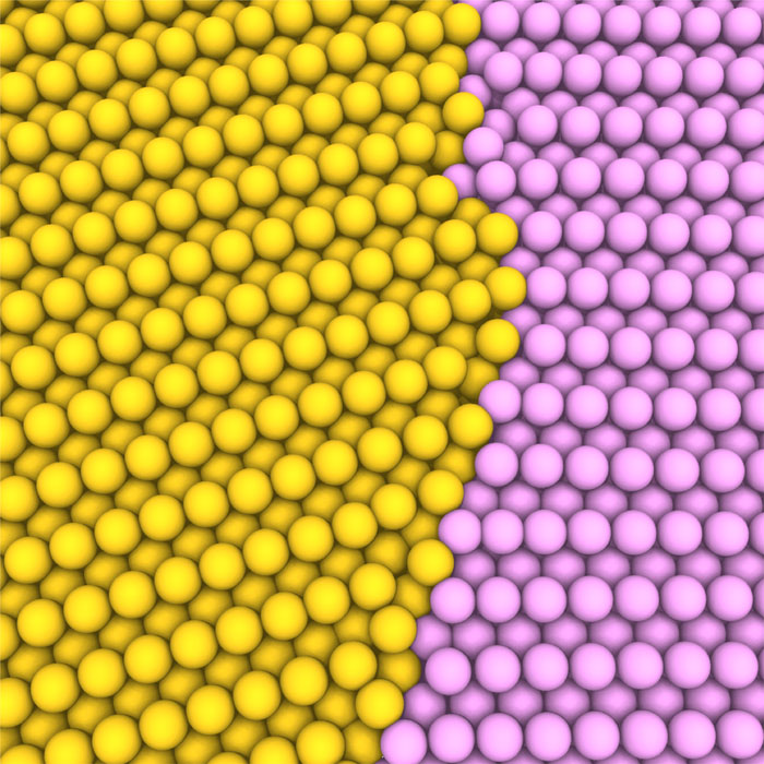
Grain boundaries are interfaces that separate different crystallographic regions, known as grains, within a polycrystalline material. In nanomaterials, grain boundaries play a crucial role in determining various physical, chemical, and mechanical properties due to the high volume fraction of interfacial regions compared to bulk materials.
Structure and Classification of Grain Boundaries
Grain boundaries can be classified based on the misorientation angle between adjacent grains:
- Low-Angle Grain Boundaries (LAGBs): LAGBs have a misorientation angle less than 15° and are composed of an array of dislocations. They have a relatively low interfacial energy and maintain a coherent structure across the boundary.
- High-Angle Grain Boundaries (HAGBs): HAGBs have a misorientation angle greater than 15° and exhibit a more disordered atomic structure. They have a higher interfacial energy and often serve as preferential sites for impurity segregation, precipitation, and corrosion.
The atomic structure at grain boundaries is influenced by factors such as the misorientation angle, the plane of the interface, and the chemical composition of the material. The disordered atomic arrangement at grain boundaries can lead to unique properties and phenomena not observed in single-crystalline materials.
Properties and Effects of Grain Boundaries
Grain boundaries significantly influence the properties of nanomaterials due to their high volume fraction and unique atomic structure. Some key effects of grain boundaries include:
Mechanical Properties
Grain boundaries can act as barriers to dislocation motion, leading to strengthening mechanisms such as Hall-Petch strengthening. However, at extremely small grain sizes (typically below 10-20 nm), grain boundaries can also facilitate grain boundary sliding and rotation, resulting in a softening effect known as the inverse Hall-Petch relation.
Diffusion and Transport
Grain boundaries provide fast diffusion pathways for atoms and ions due to their disordered structure and high density of defects. Enhanced diffusion along grain boundaries can lead to accelerated mass transport, which is important for processes such as sintering, creep, and ionic conduction in nanoionics.
Electrical and Thermal Properties
Grain boundaries can act as scattering centers for electrons and phonons, affecting the electrical and thermal conductivity of nanomaterials. The increased scattering at grain boundaries can lead to reduced electrical conductivity and enhanced thermoelectric properties, which are desirable for certain applications such as thermoelectric energy conversion.
Chemical Reactivity and Stability
The disordered atomic structure and high interfacial energy of grain boundaries make them more susceptible to chemical reactions, corrosion, and phase transformations compared to the bulk material. Grain boundary engineering can be used to control the chemical stability and reactivity of nanomaterials for specific applications.
Applications of Grain Boundary Engineering
Grain boundary engineering involves the manipulation and control of grain boundary structure, composition, and properties to optimize the performance of nanomaterials for various applications:
Nanocrystalline Metals and Alloys
Grain boundary engineering is used to enhance the mechanical properties, such as strength, ductility, and fatigue resistance, of nanocrystalline metals and alloys. By controlling the grain size distribution, grain boundary character, and segregation of solute atoms, researchers can develop high-performance structural materials for aerospace, automotive, and biomedical applications.
Ceramic and Semiconductor Nanomaterials
In ceramic and semiconductor nanomaterials, grain boundary engineering is employed to optimize electrical, thermal, and optical properties. For example, controlling the grain boundary structure and composition in thermoelectric materials can enhance the figure of merit by reducing thermal conductivity while maintaining high electrical conductivity.
Energy Storage and Conversion
Grain boundaries play a crucial role in energy storage and conversion devices, such as batteries, fuel cells, and solar cells. By engineering grain boundaries to facilitate ionic and electronic transport, researchers can improve the performance, stability, and cyclability of these devices. Nanostructured electrodes with optimized grain boundary networks can lead to higher energy and power densities in batteries and supercapacitors.
Characterization Techniques for Grain Boundaries
Several advanced characterization techniques are used to study the structure, composition, and properties of grain boundaries in nanomaterials:
- Transmission Electron Microscopy (TEM): TEM, particularly high-resolution TEM (HRTEM) and scanning TEM (STEM), provides atomic-scale imaging and analysis of grain boundary structure and composition.
- Atom Probe Tomography (APT): APT enables three-dimensional mapping of the elemental distribution at grain boundaries with near-atomic resolution, providing insights into grain boundary segregation and precipitation phenomena.
- X-ray Diffraction (XRD): XRD techniques, such as grazing incidence XRD (GIXRD) and synchrotron-based XRD, are used to characterize the average grain size, strain, and texture of nanomaterials.
- Electron Backscatter Diffraction (EBSD): EBSD is a scanning electron microscopy (SEM) based technique that provides information on grain size distribution, grain boundary misorientation, and texture of nanomaterials.
Future Perspectives
Grain boundary engineering in nanomaterials is an active area of research with immense potential for developing advanced materials with tailored properties. Future research will focus on the following aspects:
- Developing novel synthesis and processing techniques to precisely control grain boundary structure and composition in nanomaterials.
- Integrating computational modeling and machine learning approaches to predict and optimize grain boundary properties for specific applications.
- Exploring the role of grain boundaries in emerging nanomaterials, such as 2D materials, nanowires, and nanocomposites.
- Investigating the dynamic behavior of grain boundaries under extreme conditions, such as high temperature, stress, and radiation, to develop resilient nanomaterials for harsh environments.
Further Reading
Current Opinion in Solid State and Materials Science, Grain boundary segregation engineering in metallic alloys: A pathway to the design of interfaces
Beilstein Journal of Nanotechnology, A new approach to grain boundary engineering for nanocrystalline materials
