Electron Backscatter Diffraction (EBSD): Unveiling the Microstructure of Materials at the Nanoscale
What is Electron Backscatter Diffraction (EBSD)?
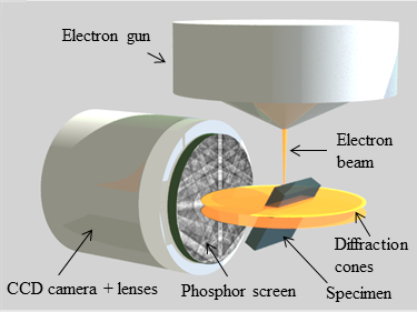
Electron backscatter diffraction (EBSD), also known as backscatter Kikuchi diffraction (BKD), is a powerful characterization technique used to analyze the microstructure, crystal orientation, and phase composition of materials at the nanoscale. EBSD is commonly performed in a scanning electron microscope (SEM) equipped with a specialized EBSD detector.
How Does EBSD Work?
In EBSD, a focused electron beam is directed at a tilted crystalline sample (usually tilted at 70° relative to the incident beam). As the electrons penetrate the sample surface, they interact with the atomic planes of the crystal lattice, causing some electrons to be backscattered. These backscattered electrons form a diffraction pattern, known as a Kikuchi pattern, on a phosphor screen positioned near the sample.
The Kikuchi pattern consists of pairs of parallel lines (Kikuchi bands) that correspond to specific crystallographic planes. The width and intensity of these bands are related to the interplanar spacing and the angle between the incident beam and the diffracting plane. By analyzing the Kikuchi patterns using specialized software, researchers can determine the crystal orientation, phase, and grain boundary characteristics at each point on the sample surface.
Key Features of EBSD
EBSD offers several unique features that make it a valuable tool for materials characterization at the nanoscale:
- High Spatial Resolution: EBSD can achieve spatial resolutions down to a few tens of nanometers, allowing for detailed analysis of nanocrystalline materials, thin films, and small-scale features.
- Orientation Mapping: EBSD enables the creation of orientation maps that visualize the crystal orientation distribution across a sample surface. These maps provide valuable insights into the texture, grain size, and grain boundary characteristics of materials.
- Phase Identification: By comparing the measured Kikuchi patterns with databases of known crystal structures, EBSD can identify the phase composition of a material, even for complex multiphase systems.
- In-situ Capabilities: EBSD can be combined with in-situ techniques, such as heating, cooling, or mechanical testing, to study the evolution of microstructure under various environmental conditions.
Applications of EBSD
EBSD finds applications in a wide range of fields, including materials science, nanotechnology, and engineering. Some key application areas include:
Microstructure Characterization
EBSD is extensively used to study the microstructure of materials, including grain size distribution, grain boundary character, and texture. This information is crucial for understanding the structure-property relationships in materials and optimizing their performance for specific applications.
Deformation and Recrystallization Studies
EBSD is a powerful tool for investigating the deformation and recrystallization behavior of materials. By mapping the crystal orientation before and after deformation or heat treatment, researchers can gain insights into the mechanisms of plastic deformation, grain growth, and phase transformations.
Nanomaterials Characterization
EBSD is increasingly applied to the characterization of nanomaterials, such as nanoparticles, nanowires, and thin films. The high spatial resolution of EBSD enables the analysis of the crystal structure, orientation, and phase distribution in these nanoscale materials, which is essential for understanding their unique properties and behavior.
Failure Analysis
EBSD is a valuable tool for failure analysis, particularly in the study of crack propagation, fatigue, and corrosion. By mapping the crystal orientation and phase distribution near failure sites, researchers can identify the microstructural factors that contribute to material failure and develop strategies for improving the durability and reliability of materials.
Challenges and Future Perspectives
Despite its numerous advantages, EBSD also faces some challenges. One of the main limitations is the need for a well-prepared, flat sample surface. Sample preparation techniques, such as mechanical polishing and ion milling, can introduce artifacts or damage the surface, which can affect the quality of EBSD results.
Another challenge is the interpretation of EBSD data, particularly for complex microstructures or multiphase materials. Advanced data processing algorithms and machine learning techniques are being developed to improve the accuracy and efficiency of EBSD data analysis.
Future developments in EBSD are expected to focus on improving the spatial and angular resolution, enhancing the speed of data acquisition, and integrating EBSD with other characterization techniques, such as transmission electron microscopy (TEM) and atomic force microscopy (AFM). The development of in-situ EBSD capabilities, such as high-temperature and high-pressure measurements, will also expand the range of applications and provide new insights into the dynamic behavior of materials at the nanoscale.
Further Reading
IOP Conference Series: Materials Science and Engineering, Advances in electron channelling contrast imaging and electron backscatter diffraction for imaging and analysis of structural defects in the scanning electron microscope
IOP Conference Series: Materials Science and Engineering, A review of EBSD: from rudimentary on line orientation measurements to high resolution elastic strain measurements over the past 30 years
