Nanowire: Definition, Synthesis, Properties, and Applications
What is a Nanowire?
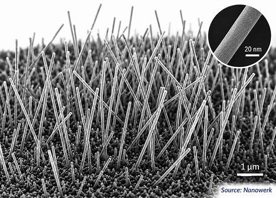
A nanowire is an extremely thin solid wire, typically about 1–100 nanometers in diameter, with a length that is hundreds to many thousands of times larger than its width.
In simple terms, a nanowire is like a crystalline thread or whisker so narrow that surfaces, interfaces, and sometimes quantum effects dominate its behavior. Nanowires belong to the broader family of nanomaterials and are one of the standard examples of one-dimensional materials: two dimensions are confined at the nanoscale, while the third extends along the wire axis.
That shape gives nanowires unusual behavior. Electrons, photons, heat, and mechanical strain are guided mainly along the wire, while the large surface-to-volume ratio makes surface chemistry and defects especially important. In very thin wires, the cross section can also be small enough to produce quantum confinement, but not every nanowire is a quantum wire.
Nanowires can be made from many materials. Common examples include silicon, germanium, gallium arsenide, indium arsenide, indium phosphide, gallium nitride, zinc oxide, silver, gold, copper, tin oxide, titanium dioxide, conducting polymers, and many compound semiconductors. The modern field grew from the vapor-liquid-solid growth of silicon whiskers described in the 1960s and expanded rapidly once catalyst particles, lithography, epitaxy, and solution methods made it possible to control wire diameters at the nanometer scale.
Key takeaways:
- A nanowire is a solid, elongated nanostructure with a nanoscale diameter and a much greater length.
- Its narrow geometry gives it one-dimensional transport pathways, a high surface-to-volume ratio, and sometimes quantum-confined electronic states.
- Nanowires are made by bottom-up growth, template methods, epitaxy, or top-down etching from wafers.
- Major uses include gate-all-around transistor concepts, photonic devices, solar cells, lithium-ion battery anodes, sensors, flexible transparent electrodes, and quantum-device research.
Structure and Geometry
The defining feature of a nanowire is its aspect ratio: it is much longer than it is wide. Many nanowires are single crystals with faceted sidewalls, although polycrystalline, amorphous, polymeric, and composite nanowires also exist. Semiconductor nanowires can contain axial or radial heterostructures, meaning that their composition can change along the length of the wire or from the core outward to the shell. These geometries are difficult to reproduce in ordinary flat thin films and are a major reason nanowires are useful in device research.
The term nanowire is sometimes confused with nearby terms. The distinctions are not always rigid, but the following comparison is useful in practice:
| Structure | Basic shape | Typical distinction |
|---|---|---|
| Nanoparticle | Compact particle | Similar dimensions in all directions |
| Nanorod | Short elongated solid | Usually only a few to about ten times longer than wide |
| Nanowire | Long elongated solid | Aspect ratio can reach hundreds, thousands, or more |
| Nanotube | Hollow elongated tube | Similar length scale to a nanowire but with an empty core |
As a wire becomes thinner, its surface becomes increasingly important. Surface oxides, adsorbed molecules, dangling bonds, and interface states can scatter carriers, change recombination rates, or shift the threshold voltage of a nanowire transistor. This sensitivity is a challenge for stable electronics but an advantage for chemical and biological sensing.
How Nanowires Are Synthesized
Nanowire synthesis falls into two broad categories. Bottom-up methods assemble wires from atoms, molecules, ions, or vapor-phase precursors. Top-down methods start with a bulk material or thin film and carve nanowires by lithography and etching.
Vapor-liquid-solid and related growth
The vapor-liquid-solid method is the classic bottom-up route. A nanoscale catalyst particle, often gold in laboratory demonstrations, absorbs vapor-phase precursors. Once the droplet becomes supersaturated, crystalline material precipitates at the droplet-substrate interface, and a nanowire grows beneath it. The catalyst particle often defines the wire diameter and remains at the tip during growth.
Related methods include vapor-solid-solid growth, solution-liquid-solid growth, oxide-assisted growth, and self-catalyzed growth, where a constituent of the target material acts as the catalyst. These approaches can produce high-quality semiconductor nanowires, including silicon, germanium, gallium arsenide, indium arsenide, gallium nitride, and zinc oxide.
Epitaxial and template-assisted growth
Molecular beam epitaxy and metal-organic chemical vapor deposition can grow nanowires at defined positions through openings in a patterned mask. This selective-area epitaxy is important for ordered arrays used in photonics, electronics, and quantum devices.
Template-assisted growth uses a porous scaffold, such as anodic aluminum oxide or a block-copolymer template. The pores are filled by electrodeposition, atomic layer deposition, sol-gel chemistry, or polymer infiltration. After the template is removed, dense arrays of metallic, oxide, polymer, or composite nanowires remain.
Top-down etching
Top-down nanowires are patterned from a wafer or film. Electron-beam lithography, nanoimprint lithography, extreme-ultraviolet lithography, reactive ion etching, and metal-assisted chemical etching can produce dense silicon nanowire arrays with controlled placement. These methods are especially attractive when nanowires must be integrated with established semiconductor manufacturing, although etched surfaces often need passivation to reduce damage and trap states.
Electronic, Optical, and Mechanical Properties
Nanowires do not all behave the same way. Their properties depend on diameter, length, crystal quality, surface chemistry, doping, contacts, strain, and surrounding environment. The common theme is that their long and narrow geometry guides transport along one direction while amplifying the influence of surfaces and interfaces.
In electronics, a nanowire can act as a narrow conducting channel. When the diameter becomes comparable to the relevant carrier wavelength, electronic states across the wire become discrete and the structure behaves as a quantum wire. This regime can produce effects such as bandgap shifts, quantized conductance, ballistic transport over short distances, and strong gate control. Larger nanowires may not be strongly quantum-confined, but they can still be valuable because their small cross section is easy to surround with an electrostatic gate.
Optically, semiconductor nanowires can absorb, scatter, guide, and emit light in ways that differ from flat films. Their diameter can support optical resonances, their length can act as a waveguide, and their end facets can form small laser cavities. Nanowire arrays can trap light efficiently while using less material, which is why they are studied for photovoltaics, LEDs, photodetectors, and nanoscale lasers.
Mechanically, many single-crystal nanowires can bend or stretch more than their bulk counterparts before failing, partly because small volumes contain fewer defects. This makes them useful as flexible electrode supports, scanning probes, resonators, strain sensors, and building blocks in stretchable or bendable devices.
Applications of Nanowires
Nanoelectronics and transistors
Nanowires are a natural geometry for gate-all-around field-effect transistors because the gate can wrap around the entire conducting channel. This improves electrostatic control and reduces leakage as transistor dimensions shrink. Commercial advanced logic has evolved from these nanowire concepts toward stacked nanosheet gate-all-around channels, which provide similar all-around gate control while offering higher drive current than a single cylindrical wire. Research nanowire devices also include tunnel FETs, memory cells, phototransistors, and nanoscale logic circuits.
Solar cells and photodetectors
Vertical nanowire arrays can improve light trapping and shorten the distance that photogenerated carriers must travel before collection. This is attractive for solar cells, photodetectors, and photoelectrochemical devices. Radial junction nanowires, where the p-n or p-i-n junction wraps around the wire, separate the direction of light absorption from the direction of carrier collection, which can help materials that absorb well but have limited carrier diffusion lengths.
Lasers, LEDs, and nanophotonics
Individual semiconductor nanowires can act as tiny optical cavities and waveguides. Zinc oxide, gallium nitride, gallium arsenide, indium phosphide, and perovskite nanowires have all been studied for nanoscale lasers and LEDs. Nanowire structures containing quantum dots are also investigated as bright single-photon emitters for quantum communication and nanophotonic circuits.
Energy storage and conversion
Silicon can store far more lithium than graphite, but bulk silicon expands dramatically during lithiation and tends to crack. Silicon-nanowire anodes address this problem by giving each wire room to expand radially while maintaining electrical contact with the current collector. Silicon-nanowire and silicon-rich composite anodes have therefore become important in high-energy lithium-ion battery development, especially where low weight is valuable.
Nanowire architectures are also studied for solid-state batteries, supercapacitors, thermoelectrics, photocatalysis, and piezoelectric nanogenerators. Zinc oxide nanowires, for example, can generate electrical signals when bent or strained, making them useful in nanoscale mechanical energy harvesting and self-powered sensor research.
Sensors and biosensors
A nanowire field-effect transistor can work as a highly sensitive chemical or biological sensor. When charged molecules bind to the nanowire surface, they change the channel conductance. Silicon, indium oxide, zinc oxide, and other nanowire nanosensors have been studied for detecting proteins, nucleic acids, viruses, gases, ions, and cellular electrical activity. The same surface sensitivity that helps detection, however, also makes reproducibility, drift, and surface passivation central engineering challenges.
Transparent electrodes and flexible electronics
Networks of silver nanowires can form transparent conducting films for touch panels, flexible displays, heaters, solar cells, and wearable electronics. The wires create conductive paths while leaving much of the area optically transparent. These networks compete with brittle transparent conductors such as indium tin oxide, especially in flexible applications.
Quantum devices and topological matter
High-mobility semiconductor nanowires, especially InAs, InSb, and Ge/Si systems, are widely used to define quantum dots, spin qubits, and hybrid semiconductor-superconductor devices. InAs and InSb nanowires with epitaxial aluminum shells are also a leading platform for proposed Majorana zero modes. This area remains scientifically active and contested: nanowires are central to the search for topological superconductivity, but experimental signatures must be carefully distinguished from non-topological effects.
Limitations and Future Perspectives
Many nanowire technologies remain difficult to scale. Bottom-up growth can produce excellent crystals, but wire diameter, length, position, composition, and crystal phase may vary from wire to wire. Top-down etching gives better placement and wafer-scale compatibility but can introduce surface damage. In both cases, contacts, passivation, alignment, packaging, and device-to-device uniformity are often harder than making a single impressive nanowire device in the laboratory.
The future of nanowires is likely to be selective rather than universal. In mainstream logic, the most commercially important descendants of nanowire research are gate-all-around nanosheet and related transistor channels. In energy storage, silicon-nanowire and silicon-rich anode designs continue to push high-energy lithium-ion cells. In photonics, sensing, and quantum devices, nanowires remain powerful research platforms because they combine small size, crystalline quality, strong surface control, and flexible heterostructure design.
FAQ: Nanowire
What is a nanowire in simple terms?
A nanowire is a solid thread only a few to a few tens of nanometers wide but much longer than it is thick. Its small diameter makes surface effects and one-dimensional transport much more important than in ordinary wires.
What is the difference between a nanowire, a nanorod, and a nanotube?
A nanorod is a short solid elongated particle, a nanowire is a much longer solid elongated structure, and a nanotube is an elongated hollow structure. In practice, the boundary between nanorod and nanowire is based mainly on aspect ratio.
How are nanowires grown?
Nanowires are grown either from the bottom up, by assembling material from vapor, solution, or template pores, or from the top down, by etching them from a wafer or film. Vapor-liquid-solid growth, selective-area epitaxy, template-assisted electrodeposition, and silicon etching are among the most common methods.
Is every nanowire a quantum wire?
No. A quantum wire is a nanowire thin and clean enough for quantum confinement to create discrete electronic states across its cross section. Many practical nanowires are too large for strong quantum confinement but still benefit from their high aspect ratio and large surface area.
Why are silicon nanowires useful in lithium-ion batteries?
Silicon can store much more lithium than graphite, but it expands strongly during charging. Nanowire geometry gives silicon room to expand without pulverizing as easily and helps maintain electrical contact during repeated cycling.
Where are nanowires used commercially?
Commercially relevant examples include silver-nanowire transparent electrodes, silicon-nanowire and silicon-rich battery anodes, and transistor architectures that evolved from nanowire gate-all-around concepts into stacked nanosheet channels. Many other uses, including nanowire solar cells, biosensors, and quantum devices, are still mainly at research or pilot scale.
Further Reading
Applied Physics Letters, Vapor-liquid-solid mechanism of single crystal growth
Nature Nanotechnology, High-performance lithium battery anodes using silicon nanowires
Nano Letters, Semiconductor nanowire: What's next?
Chemical Reviews, Vapor phase growth of semiconductor nanowires: key developments and open questions
Chemical Reviews, Electronic transport and quantum phenomena in nanowires
