Molybdenum Disulfide (MoS2): A Versatile 2D Material for Nanotechnology Applications
What is Molybdenum Disulfide (MoS2)?
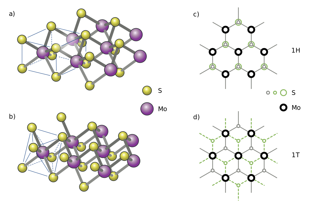
Molybdenum disulfide (MoS2) is a two-dimensional (2D) transition metal dichalcogenide (TMD) material that has gained significant attention in the field of nanotechnology due to its unique properties and diverse applications. MoS2 consists of layers of molybdenum atoms sandwiched between layers of sulfur atoms, forming a hexagonal crystal structure. The weak van der Waals interactions between the layers allow for the exfoliation of MoS2 into atomically thin nanosheets.
Properties of MoS2
MoS2 exhibits a range of remarkable properties that make it an attractive material for various nanotechnology applications:
- Electronic Properties: MoS2 is a semiconductor with a thickness-dependent bandgap. In its bulk form, MoS2 has an indirect bandgap of ~1.2 eV, which transitions to a direct bandgap of ~1.8 eV in monolayer form. This tunable bandgap makes MoS2 suitable for electronic and optoelectronic devices.
- Optical Properties: Monolayer MoS2 exhibits strong photoluminescence due to its direct bandgap, making it promising for light-emitting and photodetection applications. The optical properties of MoS2 can be further tuned by strain engineering or by creating heterostructures with other 2D materials.
- Mechanical Properties: MoS2 possesses excellent mechanical properties, with a high Young's modulus and high breaking strength. It also exhibits good flexibility and can withstand large strains without breaking, making it suitable for flexible and stretchable electronics.
- Thermal Properties: MoS2 has a high thermal conductivity, which is beneficial for heat dissipation in electronic devices. The thermal conductivity of MoS2 can be further enhanced by creating van der Waals heterostructures with other 2D materials, such as graphene.
Synthesis and Fabrication Methods
Several methods have been developed for the synthesis and fabrication of MoS2 nanomaterials:
- Mechanical Exfoliation: Mechanical exfoliation, also known as the "Scotch tape method," involves peeling off thin layers of MoS2 from a bulk crystal using adhesive tape. This method produces high-quality MoS2 flakes with pristine surfaces but is limited in terms of scalability.
- Chemical Vapor Deposition (CVD): Chemical Vapor Deposition is a scalable method for synthesizing large-area, high-quality MoS2 films. In this process, molybdenum and sulfur precursors are vaporized and deposited onto a substrate, where they react to form MoS2. CVD allows for precise control over the thickness and morphology of MoS2 films.
- Liquid-Phase Exfoliation: Liquid-phase exfoliation involves the dispersion of bulk MoS2 in suitable solvents or surfactant solutions, followed by ultrasonication or shear mixing to exfoliate the layers. This method is scalable and can produce large quantities of MoS2 nanosheets, although the resulting flakes may have a broader size distribution compared to other methods.
- Hydrothermal Synthesis: Hydrothermal synthesis is a solution-based method that involves the reaction of molybdenum and sulfur precursors in an aqueous medium at elevated temperatures and pressures. This method can produce MoS2 nanostructures with various morphologies, such as nanoflowers, nanosheets, and nanotubes.
Applications of MoS2 in Nanotechnology
MoS2 has found applications in various nanotechnology fields, leveraging its unique properties:
Electronics and Optoelectronics
MoS2 has been extensively explored for the fabrication of electronic and optoelectronic devices, such as field-effect transistors (FETs), photodetectors, and light-emitting diodes (LEDs). The thickness-dependent bandgap of MoS2 allows for the tuning of device properties, enabling the development of high-performance and energy-efficient electronic components.
Energy Storage and Conversion
MoS2 has shown great potential in energy storage and conversion applications, particularly in lithium-ion batteries and hydrogen evolution reaction (HER) catalysis. MoS2 nanosheets have been used as high-capacity anode materials in lithium-ion batteries, offering improved cycling stability and rate capability. Additionally, the edge sites of MoS2 have been found to be catalytically active for HER, making it a promising alternative to expensive platinum catalysts in hydrogen production.
Sensors and Biosensors
MoS2-based sensors and biosensors have been developed for the detection of various analytes, including gases, biomolecules, and environmental pollutants. The large surface area and high sensitivity of MoS2 nanosheets make them ideal for sensing applications. MoS2-based gas sensors have demonstrated excellent selectivity and sensitivity towards gases such as NO2, NH3, and H2S, while MoS2-based biosensors have been used for the detection of glucose, DNA, and proteins.
Challenges and Future Perspectives
Despite the significant progress in MoS2 research, several challenges need to be addressed for its widespread application. One of the main challenges is the controlled synthesis of high-quality, large-area MoS2 films with uniform thickness and minimal defects. Additionally, the integration of MoS2 with other materials, such as metal electrodes and dielectrics, needs to be optimized for the fabrication of high-performance devices.
Future research in MoS2 nanotechnology will focus on the development of novel synthesis methods, such as epitaxial growth and atomic layer deposition, to achieve precise control over the material properties. The exploration of MoS2-based heterostructures with other 2D materials, such as graphene and hexagonal boron nitride (hBN), will also be a key area of investigation for the creation of multifunctional devices with enhanced performance.
Further Reading
Inorganic Chemistry Communications, A comprehensive review on synthesis and applications of molybdenum disulfide (MoS2) material: Past and recent developments
RSC Advances, A review of molybdenum disulfide (MoS2) based photodetectors: from ultra-broadband, self-powered to flexible devices
ECS Journal of Solid State Science and Technology, Next Generation 2D Material Molybdenum Disulfide (MoS2): Properties, Applications and Challenges
