

Nanotechnology News – Latest Headlines
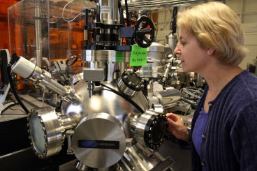
Important step toward computing with light
Research at MIT produces long-sought component to allow complete optical circuits on silicon chips.
November 23, 2011 Read more

Three-dimensional characterization of catalyst nanoparticles
In a cooperative between Helmholtz Zentrum Berlin (HZB) and the Federal Institute for Materials Research and Testing (BAM), scientists have produced the first three-dimensional representations of ruthenium catalyst particles only two nanometres in diameter using electron tomography.
November 23, 2011 Read more
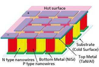
Nanowire-based generator harnesses waste energy from electronics
Researchers have created a nanoscale thermoelectric generator (TEG) using silicon nanowire arrays.
November 23, 2011 Read more
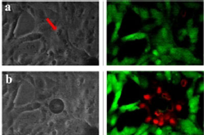
Nanomedicine: Germ killers
Polymer-based nanostructures that can selectively burst open bacteria show promise for tackling drug-resistant microbes.
November 23, 2011 Read more

Nanoparticles offer insights into interactions between single-stranded DNA and their binding proteins
Researchers have developed a convenient method to characterize the interactions between single-stranded DNA and their binding proteins.
November 23, 2011 Read more
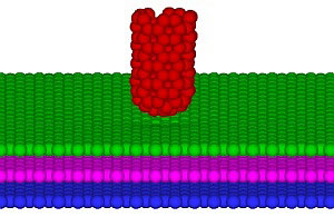
Nanotribology: Tubular probes
Short, capped single-walled carbon nanotubes may serve as ideal probing tips to study friction, lubrication and wear at the microscale.
November 23, 2011 Read more
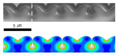
Nanowrinkles, nanofolds yield strange hidden channels
In a series of observations and experiments, engineers at Brown University and in Korea have discovered unusual properties in wrinkles and folds at the nanoscale. The researchers report that wrinkles created on super-thin films have hidden long waves that lengthen even when the film is compressed. The team also discovered that when folds are formed in such films, closed nanochannels appear below the surface, like thousands of super-tiny pipes.
November 23, 2011 Read more
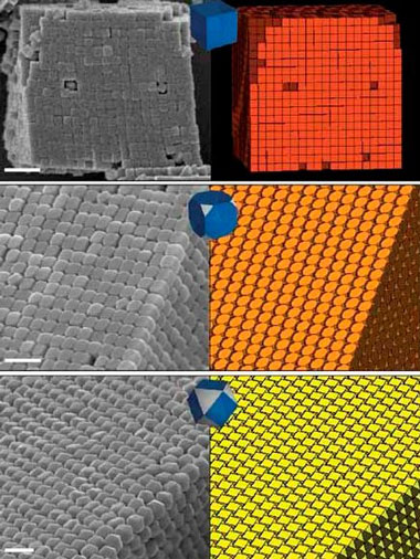
On the road to plasmonics with silver polyhedral nanocrystals
Berkeley Lab researchers find simpler approach to making plasmonic materials.
November 22, 2011 Read more
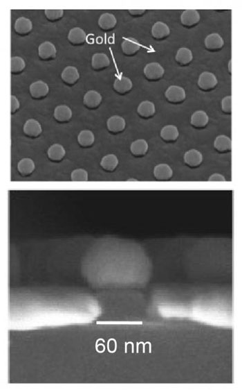
Blocked holes can enhance rather than stop light going through
Conventional wisdom would say that blocking a hole would prevent light from going through it, but Princeton University engineers have discovered the opposite to be true. A research team has found that placing a metal cap over a small hole in a metal film does not stop the light at all, but rather enhances its transmission.
November 22, 2011 Read more
The impending revolution of low-power quantum computers
Electronics could be 100 times less energy-hungry thanks to a quantum phenomenon known as the tunnel effect - by 2017 in consumer electronics.
November 22, 2011 Read more
A new practical strategy for magnetic-force-microscope cantilevers with high isotropic coercivity
A magnetic force microscope (MFM) can determine the distribution of stray fields at a level of tens of nanometers near the surface of magnetic films, and therefore is an effective tool for observing the domain structures in magnetic grains of submicrometer size.
November 22, 2011 Read more

UCSB professor receives award for graphene electronics research
Professor Kaustav Banerjee, a professor of electrical and computer engineering and Director of the Nanoelectronics Research Lab at the University of California, Santa Barbara, has been named winner of the 2011 international research award by the Electrostatic Discharge Association (ESDA).
November 22, 2011 Read more
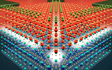
Materials scientists watch electrons "melt"
When a skier rushes down a ski slope or a skater glides across an ice rink, a very thin melted layer of liquid water forms on the surface of the ice crystals, which allows for a smooth glide instead of a rough skid. In a recent experiment, scientists have discovered that the interface between the surface and bulk electronic structures of certain crystalline materials can act in much the same way.
November 22, 2011 Read more
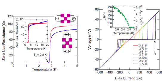
First proof of single atomic layer material with zero electrical resistance
A research group at the NIMS International Center for Materials Nanoarchitectonics (MANA) proved that the electrical resistance of a metal single atomic layer on a silicon surface becomes zero by superconductivity.
November 22, 2011 Read more
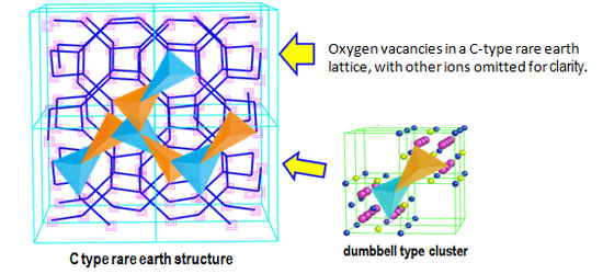
First elucidation of cause of long-term stability deterioration in solid oxide fuel cells
New research has clarified for the first time the cluster structure which has an extremely large effect on the long-term stability of solid oxide fuel cells (SOFC) for independent distributed power generation.
November 22, 2011 Read more
DARPA seeks to replace antibiotics with rapidly adaptable nanotherapeutics
Through the U.S. Department of Defense's Small Business Innovation Research (SBIR) program, DARPA is currently soliciting research proposals to develop a platform capable of rapidly synthesizing therapeutic nanoparticles targeted against evolving and engineered pathogens.
November 22, 2011 Read more
 Subscribe to our Nanotechnology News feed