-
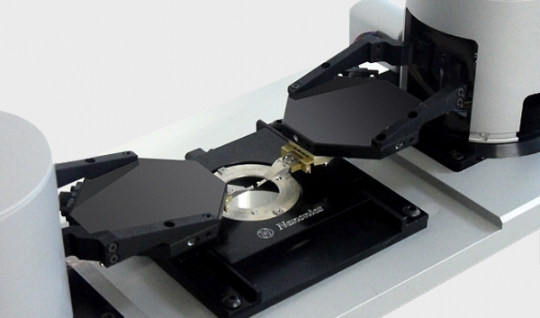
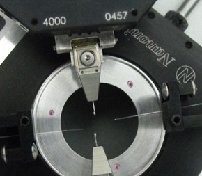
Four probes operate simultaneously and independently, with each probe having its own feedback and scanning capabilities. Measure sophisticated properties only possible with the availability of multiple probes such as electrical, thermal and optical properties of devices. The MultiView 4000 is a novel platform containing multiple probes/AFMs for advanced experiments such as: nanoscale transport, optical pump-probe, and read-write experiments. -

Nanonics Imaging Ltd. provides near-field optical microscopes (NSOM or SNOM) and atomic force microscopes (AFM). The company offers photonics and plasmonics, defect analysis solutions, dual optical microscopes, scanning stages, and scanned probe microscopy (SPM) probes and nanotools. It also provides NSOM and SPM accessories, such as liquid cells, environmental chamber and nanochemical/gas delivery systems, vibration isolation platforms, APD controllers, double APD detection systems, and NSOM and SPM heads for customized sample stages. The company’s SPM and NSOM systems comprise NSOM (SNOM) systems for transmission, collection, and true reflection NSOM imaging; Raman systems; tip-and sample-scanning probe systems for AFM/Raman/tip enhanced Raman spectroscopy and NSOM/ANSOM applications; photonics/plasmonics workstations that are designed to address nano/micro photonic characterization; fountain pen nanolithography package for chemical writing of liquids and gases; and integrated SPM with electron and ion beam microscopes. Its products are used in chemical sciences, lens characterization, life sciences, microelectronics, nanochemistry, photonics and telecommunication, physics, polymers, Raman, semiconductors, and TFT display applications. Nanonics Imaging Ltd. was founded in 1997 and is headquartered in Jerusalem, Israel.
Visit company website