High-k Dielectrics: Key to Smaller, More Efficient Semiconductors
Definition: High-k dielectrics are materials characterized by a high dielectric constant, a technical measure of a material's ability to store electrical charge in an electric field. In simpler terms, think of the dielectric constant as a way to gauge how good a material is at holding electrical energy, similar to how a sponge's quality is determined by its ability to absorb water. The higher this "sponge's" capacity, the more electrical charge it can hold, making high-k dielectrics crucial for making electronic devices smaller, faster, and more efficient.
Overview of High-k Dielectrics
In the field of semiconductor fabrication, high-k dielectrics represent a class of materials with a dielectric constant significantly higher than traditional silicon dioxide. These materials are crucial for achieving transistor scaling, enabling the reduction of gate length in transistors without increasing leakage current.
The Role of High-k Dielectrics in Semiconductor Devices
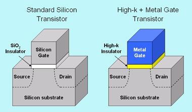
High-k dielectrics are primarily utilized in the gate dielectric layer of metal-oxide-semiconductor field-effect transistors (MOSFETs). Their high dielectric constant allows for a thicker gate oxide equivalent, critical for leakage current reduction while maintaining the electric field effect required for transistor operation.
Significance in Transistor Scaling and Semiconductor Fabrication
The advent of high-k materials has been a game-changer in semiconductor fabrication, directly addressing the challenges of transistor scaling. As devices become smaller, managing leakage current while maintaining performance becomes paramount. High-k dielectrics facilitate this balance, making them indispensable in the evolution of compact, high-performance semiconductor devices.
Advantages of Incorporating High-k Dielectrics
- Enabling Transistor Scaling: High-k materials are key to continuing Moore's Law, allowing for smaller transistor dimensions with reduced power consumption and leakage current.
- Improving Semiconductor Fabrication: They offer new pathways in semiconductor fabrication, providing solutions to traditional limitations faced by silicon dioxide and other materials.
- Leakage Current Reduction: One of the most critical advantages of high-k dielectrics is their ability to significantly reduce leakage current, enhancing device reliability and energy efficiency.
Challenges in Integration and Application
- Compatibility with Semiconductor Processes: Integrating high-k dielectrics into semiconductor fabrication processes requires careful consideration of material compatibility and process modifications.
- Advanced Deposition Techniques: Employing techniques such as atomic layer deposition (ALD) is essential for the precise application of high-k materials, ensuring uniformity and optimal performance.
Emerging High-k Materials and Their Applications
While hafnium oxide (HfO2) and zirconium oxide (ZrO2) are well-known high-k materials, recent research has expanded the list to include tantalum oxide (Ta2O5), aluminum oxide (Al2O3), and yttrium oxide (Y2O3). These materials offer different advantages in terms of dielectric properties, stability, and compatibility with semiconductor fabrication processes. Their precise application can vary, but they are primarily used to enhance transistor performance, enable further transistor scaling, and reduce leakage currents in semiconductor devices. The choice of material often depends on the specific requirements of the semiconductor fabrication process and the desired properties of the final electronic device.
Further Exploration and Learning
IEEE Transactions on Electron Devices, High-k Gate Dielectric Materials: Applications with Advanced Metal Oxide Semiconductor Field Effect Transistors (MOSFETs)
IEEE Transactions on Device and Materials Reliability, Review on high-k dielectrics reliability issues
Materials Today: Proceedings, A review on effect of various high-k dielectric materials on the performance of FinFET device
