Nanoelectromechanical Systems (NEMS): Bridging the Nano and Mechanical Worlds
Definition: NEMS (Nanoelectromechanical Systems) are smaller-scale versions of MEMS (Microelectromechanical Systems), sharing similar functional integration of electrical and mechanical components but operating at the nanometer scale for enhanced sensitivity and reduced power consumption. NEMS refer to the integration of mechanical and electrical components at the nanoscale, typically involving structures that range from 1 to 100 nanometers. These devices combine the physical properties of mechanical systems with the electronic functionality of nanoscale components, leading to unprecedented applications in sensing, actuation, and communication.
Understanding NEMS: Fundamentals and Building Blocks
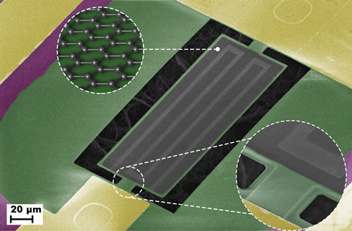
At the core of NEMS technology lies the precise fabrication of nanostructures that possess both mechanical properties and electrical functionality. These systems are developed using techniques derived from semiconductor device fabrication, including lithography, etching, and deposition, allowing for the integration of nanoscale sensors, actuators, and transducers.
Electromechanical refers to the integration and interaction between electrical and mechanical processes. In simpler terms, it's about how electronic components (like circuits) and mechanical elements (like gears or motors) work together to perform a function. At this scale, the mechanical movement could be the bending of a tiny beam, and the electrical process might involve the flow of electrons in a nano-sized circuit. This electromechanical interplay allows NEMS to perform their sophisticated tasks, such as sensing minute changes in the environment or acting as incredibly small switches for electronic signals.
How NEMS Operate
NEMS devices function by converting mechanical energy into electrical signals or vice versa. This is achieved through various mechanisms, such as capacitive sensing, piezoresistive sensing, and piezoelectric actuation. The small size of these devices enables highly sensitive detection of physical, chemical, and biological phenomena at the nanoscale. Imagine a simple example: a doorbell. When you press the doorbell button (a mechanical action), it closes an electrical circuit, sending power to ring the bell (an electrical process). This concept is fundamental in NEMS, where such interactions occur at a much smaller scale – nanometers.
Key Advantages of NEMS
- High Sensitivity: The diminutive size of NEMS allows for extraordinary sensitivity in detecting physical changes, making them ideal for applications like pressure sensing, mass detection, and chemical analysis.
- Low Power Consumption: NEMS devices require minimal power to operate due to their small mass and mechanical components, contributing to more energy-efficient systems.
- Compact Size: Their nanoscale dimensions enable the integration of NEMS into a wide range of products and technologies, including portable and wearable devices.
- Fast Response Time: The tiny mechanical elements in NEMS can move with incredible speed, leading to rapid response times in applications ranging from sensors to communication devices.
Challenges and Limitations
- Fabrication Complexity: Creating NEMS involves sophisticated and precise manufacturing techniques, making the fabrication process challenging and expensive.
- Material Behavior at Nanoscale: Materials exhibit different properties at the nanoscale, requiring extensive research to understand and optimize their performance in NEMS.
- Integration with Larger Systems: Connecting NEMS devices with macro-scale systems poses significant engineering challenges due to their size disparity.
Applications of NEMS
The potential applications for NEMS are vast and varied, touching on numerous fields:
- Healthcare and Biomedical Devices: NEMS are being explored for use in targeted drug delivery systems, biosensors, and other medical diagnostic tools due to their sensitivity and small size.
- Environmental Monitoring: These systems can detect pollutants at incredibly low concentrations, offering tools for real-time environmental monitoring and analysis.
- Communications Technology: NEMS can serve as components in the next generation of mobile devices, enabling faster and more reliable communication.
- Energy Harvesting: By converting mechanical energy from the environment into electrical energy, NEMS can power small devices, contributing to sustainable energy solutions.
Advancements and Future Directions
Innovations in fabrication technology, materials science, and computational modeling are driving the evolution of NEMS, unlocking new functionalities and applications. Ongoing research aims to address current limitations, with a focus on improving manufacturing techniques, enhancing device performance, and integrating NEMS with other nanoscale technologies.
The exploration of novel materials, such as 2D materials and nanocomposites, is also pivotal in advancing NEMS capabilities, offering the potential for even more sensitive and energy-efficient devices.
Further Reading
Materials Today: Proceedings, Review on nano-electro-mechanical-system devices
