Silicon-Vacancy (SiV) Centers: Quantum Light Sources in Diamond
What are Silicon-Vacancy (SiV) Centers?
Silicon-vacancy (SiV) centers are point defects in the crystal lattice of diamond, where a silicon atom replaces two adjacent carbon atoms. These defects act as isolated, atom-like systems embedded within the diamond matrix, exhibiting unique optical and spin properties. SiV centers have emerged as promising candidates for quantum technologies, particularly in the fields of quantum sensing, quantum communication, and quantum computing.
Structure and Formation of SiV Centers
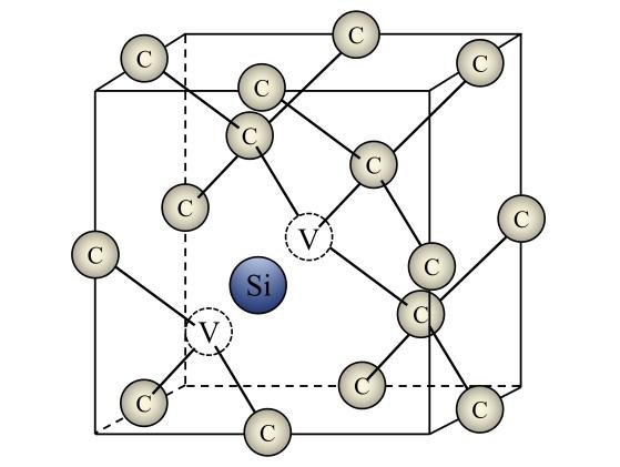
SiV centers consist of a silicon atom positioned between two vacant carbon lattice sites in diamond. The silicon atom is located at the center of a split-vacancy configuration, with the two missing carbon atoms on either side along the <111> crystallographic direction. This arrangement gives rise to the D3d symmetry of the SiV center, which plays a crucial role in its optical and spin properties.
SiV centers can be created through various methods, including:
- Ion implantation: Silicon ions are accelerated and implanted into the diamond lattice, followed by annealing to promote the formation of SiV centers.
- In-situ doping: Silicon is incorporated into the diamond lattice during the growth process, typically using chemical vapor deposition (CVD) techniques.
- Electron irradiation: High-energy electrons are used to create vacancies in the diamond lattice, which can then be filled by diffusing silicon atoms.
Optical Properties of SiV Centers
SiV centers exhibit remarkable optical properties that make them attractive for various applications:
Sharp Zero-Phonon Line (ZPL)
One of the most notable features of SiV centers is their sharp and stable zero-phonon line (ZPL) emission at 737 nm (1.68 eV). The ZPL corresponds to the direct optical transition between the ground and excited states of the SiV center, without the involvement of phonons (lattice vibrations). The narrow linewidth of the ZPL (< 1 nm at room temperature) and its insensitivity to environmental fluctuations make SiV centers ideal for quantum photonics applications.
High Quantum Efficiency
SiV centers exhibit high quantum efficiency, meaning that a large fraction of the excitation energy is converted into photons rather than being lost through non-radiative processes. This property enables efficient single-photon emission, making SiV centers promising candidates for quantum light sources and quantum communication protocols.
Optically Accessible Spin States
The electronic structure of SiV centers features optically accessible spin states, allowing for the coherent manipulation and readout of the center's spin using light. This spin-photon interface enables the realization of quantum memories, quantum repeaters, and quantum networks based on SiV centers in diamond.
Applications of SiV Centers
The unique properties of SiV centers have led to their exploration in various quantum technologies:
Quantum Sensing
SiV centers can be used as nanoscale sensors for electric and magnetic fields, temperature, and strain. Their sensitivity arises from the coupling between the center's spin and the external fields, allowing for high-resolution sensing with nanometer-scale spatial resolution.
Quantum Communication
SiV centers are promising candidates for quantum communication applications, such as quantum key distribution and quantum repeaters. Their narrow ZPL emission enables efficient coupling to optical fibers and photonic integrated circuits, while their spin-photon interface allows for the entanglement of distant SiV centers.
Quantum Computing
SiV centers can serve as quantum bits (qubits) for quantum computing. Their optically accessible spin states enable fast and high-fidelity initialization, manipulation, and readout of the qubits. The integration of SiV centers into photonic and electronic structures paves the way for scalable quantum computing architectures.
Comparison with Nitrogen-Vacancy (NV) Centers
Nitrogen-Vacancy (NV) centers are another well-studied type of color center in diamond that have been widely explored for quantum technologies. NV centers consist of a substitutional nitrogen atom adjacent to a vacant lattice site in diamond. They exhibit several similarities and differences compared to SiV centers:
Similarities
- Both NV and SiV centers are point defects in diamond that act as isolated, atom-like systems.
- They both possess optically accessible spin states, enabling spin-photon interfaces for quantum applications.
- NV and SiV centers can be used for quantum sensing, quantum communication, and quantum computing.
Differences
- NV centers have a zero-phonon line (ZPL) emission at 637 nm (1.945 eV), while SiV centers have a ZPL at 737 nm (1.68 eV).
- SiV centers exhibit a narrower and more stable ZPL compared to NV centers, making them more suitable for certain quantum photonics applications.
- NV centers typically have longer spin coherence times than SiV centers, which is advantageous for quantum sensing and quantum memory applications.
- The electronic structure and symmetry properties of NV and SiV centers differ, leading to distinct optical and spin properties.
The choice between NV and SiV centers depends on the specific requirements of the quantum application. NV centers have been more extensively studied and have demonstrated remarkable performance in quantum sensing and long-distance entanglement. On the other hand, SiV centers offer advantages in terms of their narrow and stable ZPL emission, making them promising for quantum communication and photonic integration.
Researchers are also exploring hybrid systems that combine the strengths of both NV and SiV centers. For example, coupling NV and SiV centers in diamond photonic circuits can enable the realization of quantum networks that leverage the long spin coherence of NV centers and the efficient photonic interface of SiV centers. Such hybrid approaches hold promise for the development of advanced quantum technologies that harness the complementary properties of different color centers in diamond.
Challenges and Future Perspectives
Despite the promising potential of SiV centers, several challenges need to be addressed for their widespread application:
Scalable Fabrication and Positioning
One of the main challenges is the scalable fabrication and precise positioning of SiV centers in diamond with high yield and uniformity. Current techniques, such as ion implantation and in-situ doping, often result in variations in the optical and spin properties of individual SiV centers. Developing advanced nanofabrication methods that enable deterministic placement and control over the SiV center formation process is crucial for large-scale quantum systems.
Integration with Existing Technologies
Integrating SiV centers with existing photonic and electronic technologies poses another significant challenge. Efficient coupling of SiV centers to optical cavities, waveguides, and electrical control structures is essential for realizing practical quantum devices. Overcoming issues related to material compatibility, fabrication processes, and signal transduction at the nanoscale is an active area of research.
Spin Coherence and Control
Improving the spin coherence times of SiV centers is crucial for their application in quantum computing and sensing. While SiV centers exhibit longer coherence times compared to other color centers in diamond, such as nitrogen-vacancy centers, further enhancements are necessary to perform complex quantum operations. Developing advanced dynamical decoupling techniques and identifying optimal operating conditions are key to mitigating decoherence effects.
Scalability and System Integration
Scaling up quantum systems based on SiV centers remains a significant challenge. Building large-scale quantum processors or sensor arrays requires the integration of multiple SiV centers with high fidelity and reproducibility. Addressing issues related to crosstalk, signal routing, and control complexity is essential for realizing practical quantum technologies. Developing robust and scalable architectures that can tolerate imperfections and errors is an ongoing research endeavor.
Future research directions in SiV centers include the exploration of advanced quantum protocols, such as quantum error correction and quantum algorithms, using SiV-based quantum processors. The integration of SiV centers with photonic and optoelectronic devices will enable the realization of compact and scalable quantum technologies. Furthermore, the investigation of hybrid quantum systems incorporating SiV centers and other quantum emitters or solid-state platforms will open up new avenues for quantum sensing, communication, and computing applications.
Overcoming these challenges requires a multidisciplinary approach, combining expertise from materials science, nanofabrication, photonics, and quantum information processing. Advances in these areas will pave the way for the development of practical and scalable quantum technologies based on SiV centers in diamond.
Further Reading
New Journal of Physics, Electron–phonon processes of the silicon-vacancy centre in diamond
Functional Diamond, Research Progress on Silicon Vacancy Color Centers in Diamond
Nature Photonics, Quantum technologies with optically interfaced solid-state spins
