Top-down Nanotechnology and Its Role in Nanofabrication
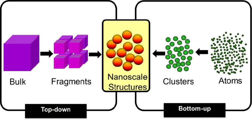
Definition: Top-down nanotechnology refers to a fabrication approach that involves the scaling down of bulk materials into nanoscale structures and devices using various methods such as lithography, etching, and milling. Contrary to the bottom-up approach, which builds materials atom by atom or molecule by molecule, top-down nanotechnology starts with larger, bulk materials and reduces them to the desired nanoscale features. This technique is widely used in semiconductor manufacturing and offers precise control over the geometry and placement of the nanoscale structures.
Core Principles and Techniques
The top-down approach relies heavily on photolithography, a process where light is used to transfer geometric patterns from a mask to a light-sensitive chemical photoresist on the substrate. Subsequent etching or material removal processes then create the desired nanostructures. Advanced techniques such as electron beam lithography and focused ion beam milling allow for even greater precision, enabling the fabrication of features down to a few nanometers in size.
How Top-down Nanotechnology Works
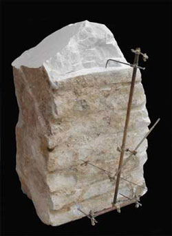
Top-down nanotechnology represents a traditional approach to nanofabrication, contrasting with the atom-by-atom assembly characteristic of bottom-up methods. This technique involves starting with a bulk material and then etching, milling, or machining it down to create nanostructures. It's a process analogous to sculpting an intricate statue from a solid block of marble, where the desired structures are carved out to achieve nanoscale dimensions.
Michelangelo's art style can be compared to a top-down approach in nanotechnology. He began with a large block of marble and gradually carved away the excess material to form his masterpieces like David.
Similarly, in nanotechnology, the top-down approach is commonly used in photolithography, which is widely employed in the semiconductor industry, and nanoimprint lithography (NIL), used in the production of nanoparticles for medical purposes. The process involves starting with a bulk material and removing unwanted bits to achieve the desired shape and size. However, this approach requires significant energy and can result in waste, while being relatively slow and challenging to replicate.

Top-down nanotechnology relies heavily on sophisticated equipment and processes to manipulate materials at the nanoscale. The approach is deterministic, meaning it follows a defined pattern or structure to remove material until the final shape is achieved. This method has been foundational in the development of semiconductor and microelectronics industries, enabling the mass production of integrated circuits and nanodevices with critical dimensions in the nanometer range.
In top-down nanofabrication, the process typically begins with a bulk material that is subsequently sculpted into nanostructures through various subtractive methods. Photolithography, along with etching (both wet and dry), is commonly employed to pattern surfaces at the nanoscale. Other techniques, like mechanical milling, can also be used to achieve desired structures, albeit with potentially less precision than lithographic methods.
Optical lithography and nanoimprint lithography (NIL) stand out as the predominant methods in top-down nanomanufacturing, supported by a variety of other nanofabrication techniques. Optical lithography, a mainstay in the semiconductor industry, uses light to transfer a geometric pattern from a photomask to a light-sensitive chemical photoresist on the substrate. NIL, on the other hand, physically presses a mold with nanostructures into a substrate to create the desired patterns.
Electron beam lithography (EBL) showcases the ability to produce features smaller than 10 nm across large areas, achieving precise placement and overlay. However, its commercial applications are somewhat limited due to lower throughput, primarily being utilized for mask production in photolithography and NIL, as well as in device development.
Key Advantages of Top-down Nanotechnology
Top-down nanotechnology offers several significant benefits:
- Precise Control Over Structures: Allows for accurate patterning and placement of nanoscale features, critical for semiconductor and microelectronic applications.
- Compatibility with Existing Manufacturing Processes: Easily integrates into the current semiconductor manufacturing infrastructure, facilitating rapid adoption and implementation.
- High Yield: Capable of producing a large number of devices in parallel, which is essential for commercial-scale production.
Limitations and Challenges
Despite its advantages, top-down nanotechnology faces certain challenges:
- Physical and Chemical Limitations: The further reduction in size is limited by the physical properties of the materials and the resolution of lithography techniques.
- Cost: High energy consumption and the need for expensive, sophisticated equipment can drive up costs, particularly for ultra-high precision requirements.
- Material Waste: The subtractive nature of the processes can lead to significant material waste compared to bottom-up approaches.
Applications of Top-down Nanotechnology
Top-down nanotechnology is pivotal in several key industries:
- Microelectronics and Semiconductors: The manufacturing of integrated circuits (ICs) and microprocessors relies on top-down techniques to create the complex patterns required for electronic components.
- Data Storage: Techniques such as nanolithography are employed to increase the density of data storage devices, allowing for more compact and high-capacity memory devices.
- Sensors and Diagnostics: Fabrication of nanoscale sensors that can detect minute quantities of chemicals or biological agents, useful in medical diagnostics and environmental monitoring.
- Optics and Photonics: Production of nanostructured materials that manipulate light at the nanoscale for applications in lenses, mirrors, and other optical components.
Comparative Insights with Bottom-Up Approaches
While top-down nanotechnology excels in precision and integration with current manufacturing processes, bottom-up approaches offer advantages in terms of material diversity and potential for novel properties through self-assembly. The choice between top-down and bottom-up methods depends on the specific application requirements, including the desired material properties, complexity, and cost constraints.
The Future of Top-down Nanotechnology
As the demand for smaller, faster, and more energy-efficient devices continues to grow, the role of top-down nanotechnology in enabling these advancements remains critical. Ongoing research and development are focused on overcoming the existing limitations, such as improving lithography techniques for better resolution and reducing costs, to ensure that top-down nanofabrication continues to drive innovation in nanotechnology and beyond.
Further Reading
Advances in Colloid and Interface Science, "Advances in top–down and bottom–up surface nanofabrication: Techniques, applications & future prospects"
Advances in Colloid and Interface Science, "Synthesis of nanomaterials using various top-down and bottom-up approaches, influencing factors, advantages, and disadvantages: A review"
