| Posted: Jun 13, 2014 |
Nano-imaging probes molecular disorder |
| (Nanowerk News) Using a newly developed imaging method, researchers show that thin-film organic semiconductors contain regions of structural disorder that could inhibit the transport of charge and limit the efficiency of organic electronic devices. |
| Semiconductors based on organic polymers or small molecules have several advantages over their conventional, mostly silicon-based cousins. They are simpler and cheaper to manufacture, and can be produced in the form of thin, flexible layers, which allows them to be attached to diverse substrates and surfaces. This versatility means that organic semiconductors are of great interest for a wide range of applications – including optoelectronic devices such as light-emitting diodes and solar cells. Their electrical conductivity and energy efficiency are a function of the properties of the materials of which they are made. This is why LMU researchers led by Dr. Bert Nickel have been investigating how the degree of molecular order within organic thin films affect the mobility and transport of the charge carriers within them. |
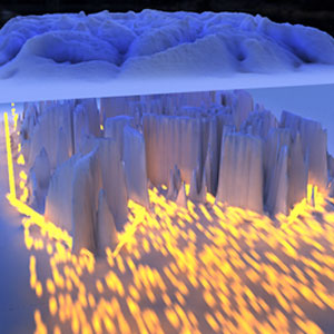 |
| A 3-D depiction of the newly discovered inclusions. The yellow lines represent the scattering of charge carriers at inclusion boundaries. (Source: Christoph Hohmann, NIM) |
| In semiconductor-based components, the mobility of the charge-carrying particles – electrons and their positively charged counterparts, known as holes – should be as high as possible. “There have been conflicting reports concerning the effect of the granularity and crystallinity of the organic semiconducting thin film on the separation and transport of charge carriers inside,” says Nickel. He and his colleagues have now taken a closer look at the molecular structure of a thin film of pentacene, a prototype organic semiconductor. |
| Bringing the structure into focus |
| “Nanoscale studies like this are very challenging“, says LMU physicist Dr. Fritz Keilmann, a pioneer in the field of near-field microscopy. “We have been successful because we have developed a laser-based, high-resolution imaging method at Neaspec GmbH, a spin-off from the Center for NanoScience at LMU. We illuminate the extremely fine tip of an atomic force microscope with a focused infra-red laser beam. The tip acts as a nano-antenna and converts the incident radiation into an intense near-field light source with a diameter of about 20 nanometers. This suffices to provide a high-precision analysis of the structure of the semiconducting film – which reveals the spatial arrangement of its component molecules.” |
| To everyone’s surprise, the experiments showed that, while the flat grains of pentacene that make up the thin organic film often appear homogeneous over large regions, these areas are interrupted by inclusions in which the pentacene molecules are ordered in a different pattern or crystalline phase. “In these areas, the pentacene molecules are more strongly tilted than those in neighboring regions. We suspect that these inclusions inhibit charge-carrier transport in the organic layer, rather like rocks in a river perturb the flow of water,” says Christian Westermeier, first author on the study ("Sub-micron phase coexistence in small-molecule organic thin films revealed by infrared nano-imaging"). |
| Differences in crystal structure on extremely short scales are not only relevant to the operation of high-conductivity electronic components such as the transistor element investigated in this new study. They also play a crucial role in organic solar cells, which are made up of several such molecular layers. “Up until now, it has been very difficult to access these structures experimentally. So our method can make a valuable contribution to our understanding of these layered systems and to organic electronics in general,” Nickel concludes. |
| Source: By Monika Gödde, Ludwig-Maximilians Universität München |

