| Posted: Nov 12, 2014 |
OLED devices for lab-on-a-chip-applications |
| (Nanowerk News) Smart and portable medical equipment is essential for fast and easy point-of-care and point-of-use diagnostics. Lab-on-a-chip applications in hand-held devices can help to save time for laboratory medical analysis in emergency scenarios. The combination of sub-micrometer-thick light emitting devices and photo-detectors with tunable spectral characteristics could play a key role in future sensing chips based on organic electronics. |
| These applications realize the excitation and detection of fluorescence or phosphorescence in a marker. Even time-resolved measurements are possible. The integration of both, OLED together with organic photodiodes into one chip could be a way to achieve low-cost personal diagnostics outside the laboratory. |
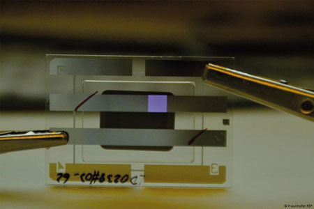 |
| UV-OLED (Image: Fraunhofer) |
| At IDW 2014 Fraunhofer FEP presents two different OLED-device concepts: one emitting in the near UV and another one in the green spectral range which both could be integrated to sensor applications. |
| These two exemplary OLED developments can be used for biomedical and biotechnical sensing in lab-on-chip applications. Near ultra-violet emission from an OLED is demonstrated for bottom- as well as from top-emitting device architectures. Furthermore, the scientists from Fraunhofer FEP combined a green top-emitting OLED with a thin-film optical filter and thin-film encapsulation so that a sample substance can be brought in proximity to the excitation source. Both developed devices are suitable for large area deposition and integration on silicon-backplanes like wafers as light source for optical excitation to detect fluorescence or phosphorescence signals. |
| Dr. Michael Thomschke, project leader at Fraunhofer FEP states: “These developments could be incorporated in very small ultra-thin organic devices based on glass, foil or opaque silicon-backplanes. The integration e.g. on silicon-wafers could be very cost-efficient. The corresponding processes allow large area manufacturing as well as devices in the µm scale.” |
| Later on, such device could be extended with microfluidics or external optics to fit a certain application. |
| Next to the results for for OLED applications using UV-electroluminescence, Fraunhofer FEP will also present further demonstrators of our latest OLED microdisplays and flexible OLED on different substrates at our booth during the conference. |
| Besides the exhibition Dr. Michael Thomschke will give a talk „OLED on Silicon for Sensor Applications“ about the latest approaches of OLED devices for lab-on-a-chip applications on Wednesday, December 3, 15:45 – 16:05 in Snow Hall B. |
| Source: Fraunhofer Institute for Organic Electronics, Electron Beam and Plasma Technology |

