| Posted: Jul 26, 2016 |
A graphene window to better microfluidics
(Nanowerk News) Working with protein microcrystals can be an enormously challenging endeavor. Aside from their extremely small size, microcrystals can be delicate, difficult to handle, and susceptible to radiation damage from x-ray diffraction studies. Microfluidic lab-on-a-chip technologies offer some highly promising ways to circumvent these difficulties, but can bring with them new problems to overcome.
|
|
A team of experimenters from the University of Massachusetts Amherst and The University of Chicago utilized high-brightness x-rays from the U.S. Department of Energy’s Advanced Photon Source (APS) at Argonne as they developed a new strategy to combat these limitations by combining microfluidics with another cutting-edge technology, single-layer graphene, for serial protein crystallography in an ultrathin microfluidic chip.
|
|
Their work was published in Lab On a Chip ("Graphene-based microfluidics for serial crystallography").
|
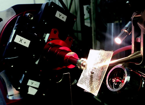 |
| Fig. 1. A microbatch-style graphene-based microfluidic chip mounted at the 14-ID-B station at the APS.
|
|
In serial crystallography, protein crystals are characterized by combining data from many smaller crystals to provide a complete dataset. Microfluidic or nanofluidic devices can make this process much easier and more efficient than bulk crystallization techniques, providing an environment in which hundreds or even thousands of microcrystals can be grown under precisely controlled conditions and preserved for long periods.
|
|
But there are nagging problems with this process, among them the inevitable attenuation of the x-ray beam as it passes through the microfluidic device, which is generally made of glass, plastic, or PDMS (poly(dimethylsiloxane)) material. Creating thinner devices that are more amenable to x-ray transmission is technically difficult and can allow the loss of water with subsequent sample dehydration.
|
|
These are the issues that the research team sought to overcome.
|
|
Inspired by recent work in which a graphene layer wrapping was shown to protect protein crystals from dehydration with only limited beam attenuation, the team fashioned a thin film of graphene and a support layer of PMMA (poly(methylmethacrylate)) for use as a diffusion barrier in a microfluidic chip. Including this combined ~1 µm-thick PMMA/graphene window, the chip comprised five layers, with microfluidic channels cut into a ~100 µm-thick COC (cyclic olefin copolymer) film.
|
|
The experimenters examined the composition and quality of the device using Raman spectroscopy, permeability measurements, and atomic force microscopy, all of which confirmed the structure of the microchip.
|
|
As a practical demonstration of the advantages of graphene-based microfluidics, the researchers used their device to determine the crystal structure of hen egg white lysozyme (HEWL). They conducted x-ray diffraction studies at the BioCARS 14-ID-B beamline at the APS, collecting multiple data frames at different beam angles using a polychromatic, 12-keV x-ray beam (Fig. 1). |
|
With the graphene layer doing double duty as both an x-ray window with low beam attenuation and high signal-to-noise, and also as a diffusion barrier to prevent evaporation, the research team performed microbatch and counter-diffusion crystallization trials with the HEWL model system. Crystals formed easily and quickly inside the device and remained stable for days to weeks afterward, remaining undisturbed even after they were shipped from the lab to the APS facility for study.
|
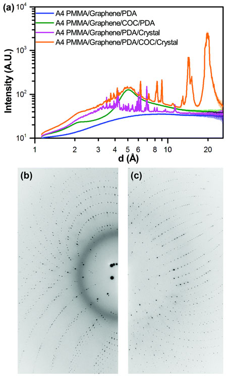 |
| Fig. 2. (a) One-dimensional integrated x-ray intensity profiles showing the relative strength of the observed diffraction signal from a HEWL crystal compared to the noise resulting from background scattering due to the presence of device materials as a function of resolution. The corresponding two-dimensional diffraction images for the (b) A4 PMMA/graphene/PDA/COC/crystal dataset (orange), and the (c) A4 PMMA/graphene/PDA/crystal dataset (magenta) shown in (a).
|
|
Observations of background scattering and signal-to-noise (Fig. 2) showed that both were excellent, particularly in comparison to previous mounting strategies for serial crystallography, which were approximated for these experiments by collecting data on crystals through a ~100 µm-thick COC layer.
|
|
The high quality of data was maintained even when considering variations in the incidence angle of the x-ray beam resulting from variations in sample orientation. The experimenters' device displayed a signal transmission of 99.9% even up to a +/-55° rotation, compared to previously reported PDMS/COC-bas
|
|
ed chips where a maximum of 77% transmission could only be achieved in the absence of rotation. High-quality, high-resolution images and diffraction data were obtained in various configurations compared to microfluidic devices constructed of more traditional materials.
|
|
The investigators plan to expand upon this work with further experiments to enable structure determination of novel protein targets and ultimately time-resolved structural studies of protein dynamics.
|
|
Although the present research concentrates on protein crystallography, they emphasize that their strategies for microfluidic device fabrication could have broad applications across many other disciplines, including DNA analysis and microarrays, pathology and medical diagnostics, nanotechnology, biophysics—essentially every field that makes use of microfluidics and lab-on-a-chip technologies.
|

