| Jan 17, 2019 |
Creating a roadmap for 2D materials(Nanowerk News) The rapid growth of research on 2D materials – materials such as graphene and others that are a single or few atoms thick – is fueled by the hope of developing better performing sensors for health and environment, more economical solar energy, and higher performing and more energy efficient electronics than is possible with current silicon electronics. |
| Technical roadmaps, such as the International Technology Roadmap for Semiconductors (ITRS), first published in 1998, serve as guides for future advances in a particular field and provide a means for organizations to plan for investments in new technology. |
| An invited article in the journal 2D Materials ("A roadmap for electronic grade 2D materials") provides a roadmap for the synthesis of electronic-grade two-dimensional materials for future electronic and sensing applications. Led by Penn State, with contributions from five additional universities and national laboratories, the roadmap addresses the grand challenges in 2D materials with useful electronic or photonic properties, and the outlook for U.S. advances in the field. |
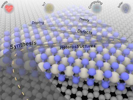 |
| A roadmap for 2D materials explores the challenges of synthesizing electronic grade materials. (Image: Natalie Briggs/Penn State) |
| “This article is a review of where we currently are in regard to the synthesis of 2D materials and our thoughts on the top research priorities that need to be addressed to achieve electronic grade 2D materials,” said Joshua Robinson, associate professor of materials science and engineering, whose Ph.D. students Natalie Briggs and Shruti Subramanian are co-lead authors on the report titled “A Roadmap for Electronic Grade 2-Dimensional Materials,” published online today, Jan. 17. |
| “2D materials are touted to be revolutionary for a variety of technologies, assuming the materials are perfect,” he said. “But that’s never the case – we have a long way to go before the materials are perfect. Our hope is that the roadmap provides a guide to get us there. Once that happens, the technology can really take off.” |
| The authors divided the paper into four parts: Grand Challenges, which are the technology drivers, such as the internet of things; Synthesis, the techniques and theories required to grow close to perfect 2D materials; Materials Engineering, which is fine tuning the properties of 2D and composite materials; and finally, Outlook, which is the future of electronic devices when silicon technology reaches an inevitable roadblock. |
| “To put our roadmap together, we reached out to experts in various subfields, such as different synthesis approaches, defect engineering and computational theory,” said Briggs of the two-year project. “We asked them to talk about the key fundamental challenges and the steps required to address these challenges in their area of expertise.” |
| Robinson added, “This is the first roadmap focused on 2D synthesis for electronic applications and there are still a lot of open questions. We want to bring some of those topics into the light.” |
| Source: Penn State Materials Research Institute |
|
Subscribe to a free copy of one of our daily Nanowerk Newsletter Email Digests with a compilation of all of the day's news. |

