| May 28, 2019 |
Taking the guesswork out of electrospinning(Nanowerk News) Electrospinning, a nanofiber fabrication method, can produce nanometer- to micrometer-diameter ceramic, polymer, and metallic fibers of various compositions for a wide spectrum of applications: tissue engineering, filtration, fuel cells and lithium batteries. These materials have unique properties because of their high-aspect-ratio morphology and large surface area. |
| Yet their development has largely been by trial and error, making it difficult to reproduce reliably in industrial settings. This challenge stems from a lack of understanding of the underlying dynamics during the process, which involves more than 10 control parameters. |
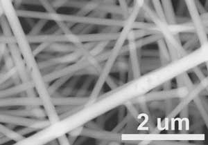 |
| Electrospun fibers have a high surface-area-to-volume ratio, which favors surface reaction applications like catalysts, and superior mechanical properties compared with their bulk counterparts, making them less subject to mechanical failure. (Image: Argonne National Laboratory) |
| The U.S. Department of Energy’s (DOE) Argonne National Laboratory is taking the guesswork out of electrospinning by leveraging its unique suite of capabilities to build a database that correlates electrospinning machine parameters with nanofiber properties. The suite will allow companies to design materials optimized for specific applications at top speed, while also making possible real-time feedback and control on the manufacturing floor. |
| The advanced electrospinning facility is part of Argonne’s advanced manufacturing science and engineering effort to accelerate materials development and manufacturing processes by developing platform technologies augmented with state-of-the-art computing and diagnostics systems. This combination enables predictive science that reduces costly trial-and-error prototyping. The project is funded by Argonne’s manufacturing Laboratory-Directed Research and Development (LDRD) program. |
| Argonne is in a unique position to advance electrospinning technology because of a combination of expertise in materials development and scaleup, along with the unique diagnostic capabilities available at the Advanced Photon Source (APS), a DOE Office of Science User Facility and the nation’s highest-energy synchrotron X-ray source. |
| The researchers, led by Argonne materials scientist Yuepeng Zhang, are conducting in-situ X-ray measurements at the 12 ID-B beamline at the APS. The measurements capture real-time structural, physical and chemical information from nanofibers as they form and change during processing, facilitating correlation with processing parameters (e.g., voltage, working distance and precursor viscosity). |
| According to Zhang, “The measurements provide — for the first time — a systematic understanding of the spinning and annealing processes to control and enhance product performance.” |
| The next step is to enter the X-ray data into machine-learning algorithms that run on high-performance computing facilities at Argonne. These computations will further optimize speed, reduce material defects, predict novel properties and eliminate costly trial-and-error prototyping. |
| The electrospinning capability also can be adapted for use with roll-to-roll manufacturing processes (which involve continuous processing of a flexible substrate as it’s transferred between two moving rolls of material) to accelerate commercialization and reduce costs. Argonne is demonstrating the roll-to-roll concept and its first application by producing large-area LLZO solid-state electrolytes for energy storage applications. |
| Industry can collaborate with experts at Argonne to develop electrospinning processes for their existing materials, as well as collaborate on new or emerging (composite) materials and designs, including scaleup. |
| To collaborate on designing and scaling materials with Argonne’s electrospinning system, contact Yuepeng Zhang at [email protected]. |
| Key applications for electrospun materials: |
|
|
| Benefits of electrospinning: |
|
|
| Source: Argonne National Laboratory |
|
Subscribe to a free copy of one of our daily Nanowerk Newsletter Email Digests with a compilation of all of the day's news. |

