| Aug 14, 2019 |
Thinnest optical waveguide channels light within just three layers of atoms(Nanowerk News) Engineers at the University of California San Diego have developed the thinnest optical device in the world—a waveguide that is three layers of atoms thin. |
| The work is a proof of concept for scaling down optical devices to sizes that are orders of magnitude smaller than today’s devices. It could lead to the development of higher density, higher capacity photonic chips. Researchers published their findings in Nature Nanotechnology ("Guiding of visible photons at the ångström thickness limit"). |
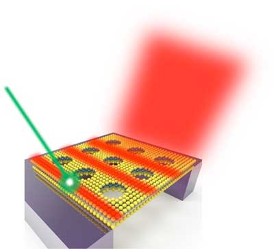 |
| Illustration of a tungsten disulfide monolayer suspended in air and patterned with a square array of nanoholes. Upon laser excitation, the monolayer emits photoluminescence. A portion of this light couples into the monolayer and is guided along the material. At the nanohole array, periodic modulation in the refractive index causes a small portion of the light to decay out of the plane of the material, allowing the light to be observed as guided mode resonance. (Image: Cubukcu lab) |
| “Fundamentally, we demonstrate the ultimate limit for how thin an optical waveguide can be built,” said senior author Ertugrul Cubukcu, a professor of nanoengineering and electrical engineering at UC San Diego. |
| The new waveguide measures about six angstroms thin—that is more than 10,000 times thinner than a typical optical fiber and about 500 times thinner than on-chip optical waveguides in integrated photonic circuits. |
| The waveguide consists of a tungsten disulfide monolayer (made up of one layer of tungsten atoms sandwiched between two layers of sulfur atoms) suspended on a silicon frame. The monolayer is also patterned with an array of nanosized holes forming a photonic crystal. |
| What’s special about this monolayer crystal is that it supports electron-hole pairs, known as excitons, at room temperature. These excitons generate a strong optical response, giving the crystal a refractive index that is about four times greater than that of air, which surrounds its surfaces. By comparison, another material with the same thickness would not have as high of a refractive index. When light is sent through the crystal, it is trapped inside and guided along the plane by total internal reflection. This is the basic mechanism for how an optical waveguide works. |
| Another special feature is that the waveguide channels light in the visible spectrum. “This is challenging to do in a material this thin,” Cubukcu said. “Waveguiding has previously been demonstrated with graphene, which is also atomically thin, but at infrared wavelengths. We’ve demonstrated for the first time waveguiding in the visible region.” |
| Nanosized holes etched into the crystal allow some light to scatter perpendicular to the plane so that it can be observed and probed. This array of holes produces a periodic structure that makes the crystal double as a resonator as well. |
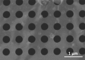 |
| SEM image of the waveguide structure: a suspended tungsten disulfide monoloayer patterned with nanosized holes. (Image: Cubukcu lab) |
| “This also makes it the thinnest optical resonator for visible light ever to be demonstrated experimentally,” said first author Xingwang Zhang, who worked on this project as a postdoctoral researcher in Cubukcu’s lab at UC San Diego. “This system does not only resonantly enhance the light-matter interaction, but also serves as a second-order grating coupler to couple the light into the optical waveguide.” |
| Researchers used advanced micro- and nanofabrication techniques to create the waveguide. Creating the structure was particularly challenging, said Chawina De-Eknamkul, a nanoengineering PhD student at UC San Diego and a co-author of the study. “The material is atomically thin, so we had to devise a process to suspend it on a silicon frame and pattern it precisely without breaking it,” she said. |
| The process starts with a thin silicon nitride membrane supported by a silicon frame. This is the substrate upon which the waveguide is built. An array of nanosized holes is patterned into the membrane to create a template. Next, a monolayer of tungsten disulfide crystal is transferred onto the membrane. Ions are then sent through the membrane to etch the same pattern of holes into the crystal. In the last step, the silicon nitride membrane is gently etched away, leaving the crystal suspended on the silicon frame. The result is an optical waveguide in which the core consists of a monolayer tungsten disulfide photonic crystal surrounded by a material (air) with a lower refractive index. |
| Moving forward, the team will continue to explore the fundamental properties and physics pertaining to the waveguide. |
| Source: University of California San Diego |
|
Subscribe to a free copy of one of our daily Nanowerk Newsletter Email Digests with a compilation of all of the day's news. |

